Display
A display and display area technology, applied in the direction of instruments, nonlinear optics, optics, etc., can solve problems such as poor display and achieve good reliability
- Summary
- Abstract
- Description
- Claims
- Application Information
AI Technical Summary
Problems solved by technology
Method used
Image
Examples
no. 1 example
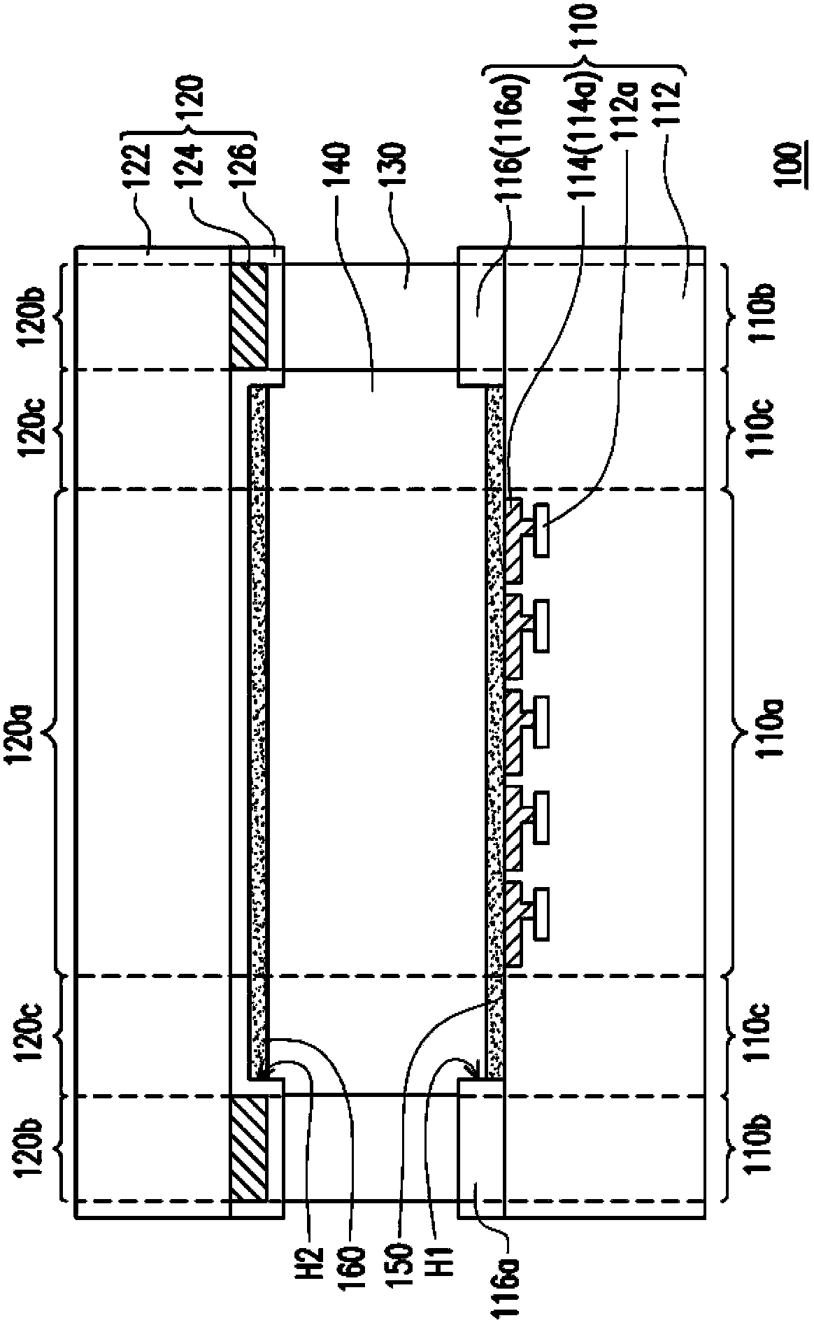
[0067] figure 1 It is a schematic cross-sectional view of the display according to the first embodiment of the present invention. Please refer to figure 1 , the display 100 of this embodiment includes a first substrate 110, a second substrate 120 opposite to the first substrate 110, a sealant 130 between the first substrate 110 and the second substrate 120, a liquid crystal layer 140, and a first alignment Film 150. The first substrate 110 , the second substrate 120 and the sealant 130 surround the liquid crystal layer 140 together. The sealant 130 of this embodiment is used to join the first substrate 110 and the second substrate 120 . The sealant 130 of this embodiment can be heat-curable glue, ultraviolet-curable glue, or other suitable types of glue. The liquid crystal layer 140 in this embodiment is used as a light valve, thereby enabling the display 100 to display images. The liquid crystal material selected for the liquid crystal layer 140 in this embodiment can be...
no. 2 example
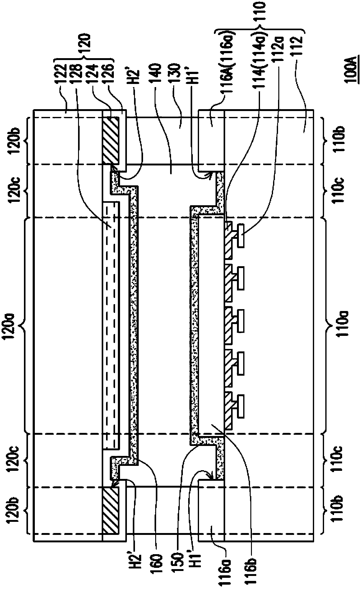
[0076] figure 2 It is a schematic cross-sectional view of the display device according to the second embodiment of the present invention. Please refer to figure 2 , the display 100A of this embodiment is similar to the display 100 of the first embodiment, so the same components are denoted by the same reference numerals. The difference between the display 100A of this embodiment and the display 100 of the first embodiment is as follows: the area covered by the first recess H1' of this embodiment is different from that of the first recess H1 of the first embodiment. The area covered by the first protective pattern layer 116A in this embodiment is different from that of the first protective pattern layer 116 in the first embodiment. The second substrate 120A of this embodiment further includes a second protection pattern layer 128 . In addition, the area covered by the second recess H2' of this embodiment is also different from that of the second recess H2 of the first embo...
no. 3 example
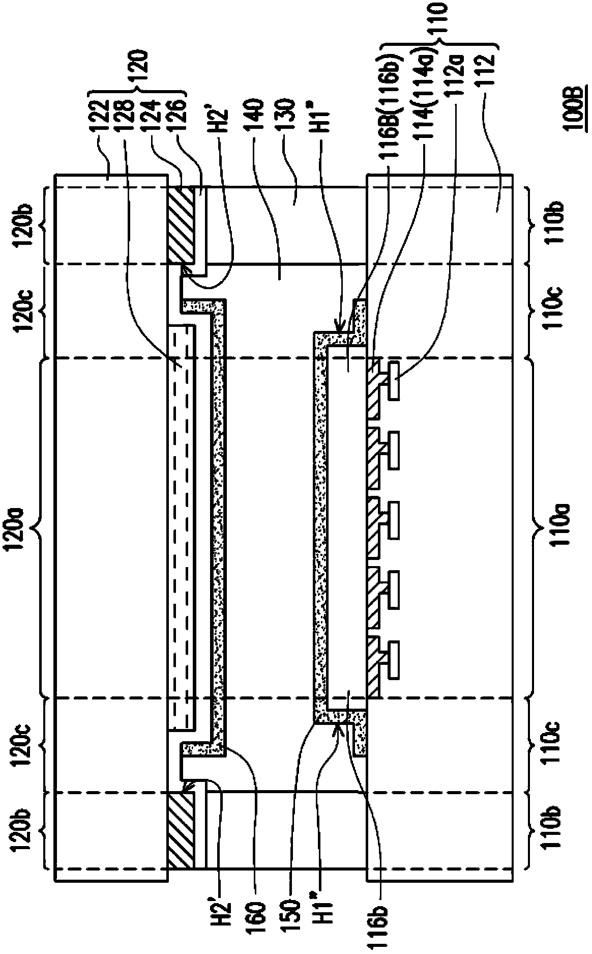
[0081] image 3 It is a schematic cross-sectional view of a display device according to a third embodiment of the present invention. Please refer to image 3 , the display 100B of this embodiment is similar to the display 100A of the second embodiment, so the same components are denoted by the same reference numerals. The difference between the display 100B of this embodiment and the display 100A of the second embodiment lies in that the area covered by the first depression H1 ″ of this embodiment is different from that of the first depression H1 ′ of the second embodiment. In addition, the The form of the first protection pattern layer 116B is slightly different from that of the first protection pattern layer 116A of the second embodiment. The differences between the two will be described below, and the similarities between the two will not be repeated.
[0082] Please refer to image 3 In this embodiment, the first substrate 110 includes a silicon substrate 112 , a pixel ...
PUM
 Abstract
Description
Claims
Application Information
 - R&D Engineer
- R&D Manager
- IP Professional
- Industry Leading Data Capabilities
- Powerful AI technology
- Patent DNA Extraction
Browse by: Latest US Patents, China's latest patents, Technical Efficacy Thesaurus, Application Domain, Technology Topic, Popular Technical Reports.
© 2024 PatSnap. All rights reserved.Legal|Privacy policy|Modern Slavery Act Transparency Statement|Sitemap|About US| Contact US: help@patsnap.com


