Solid-state imaging device and manufacturing method therefor
A solid-state imaging device and semiconductor technology, which is applied in the direction of electric solid-state devices, radiation control devices, semiconductor devices, etc., can solve problems such as white spots, poor crystal quality, and poor semiconductor layers, and achieve the effect of improving sensitivity
- Summary
- Abstract
- Description
- Claims
- Application Information
AI Technical Summary
Problems solved by technology
Method used
Image

Examples
no. 1 Embodiment approach
[0099] refer to Figure 1 to Figure 4 , the solid-state imaging device according to the first embodiment of the present invention will be described. In addition, this invention is not limited to the following embodiment. In addition, appropriate changes can be made without departing from the range in which the effects of the present invention are achieved. Furthermore, each embodiment can also be combined with other embodiment.
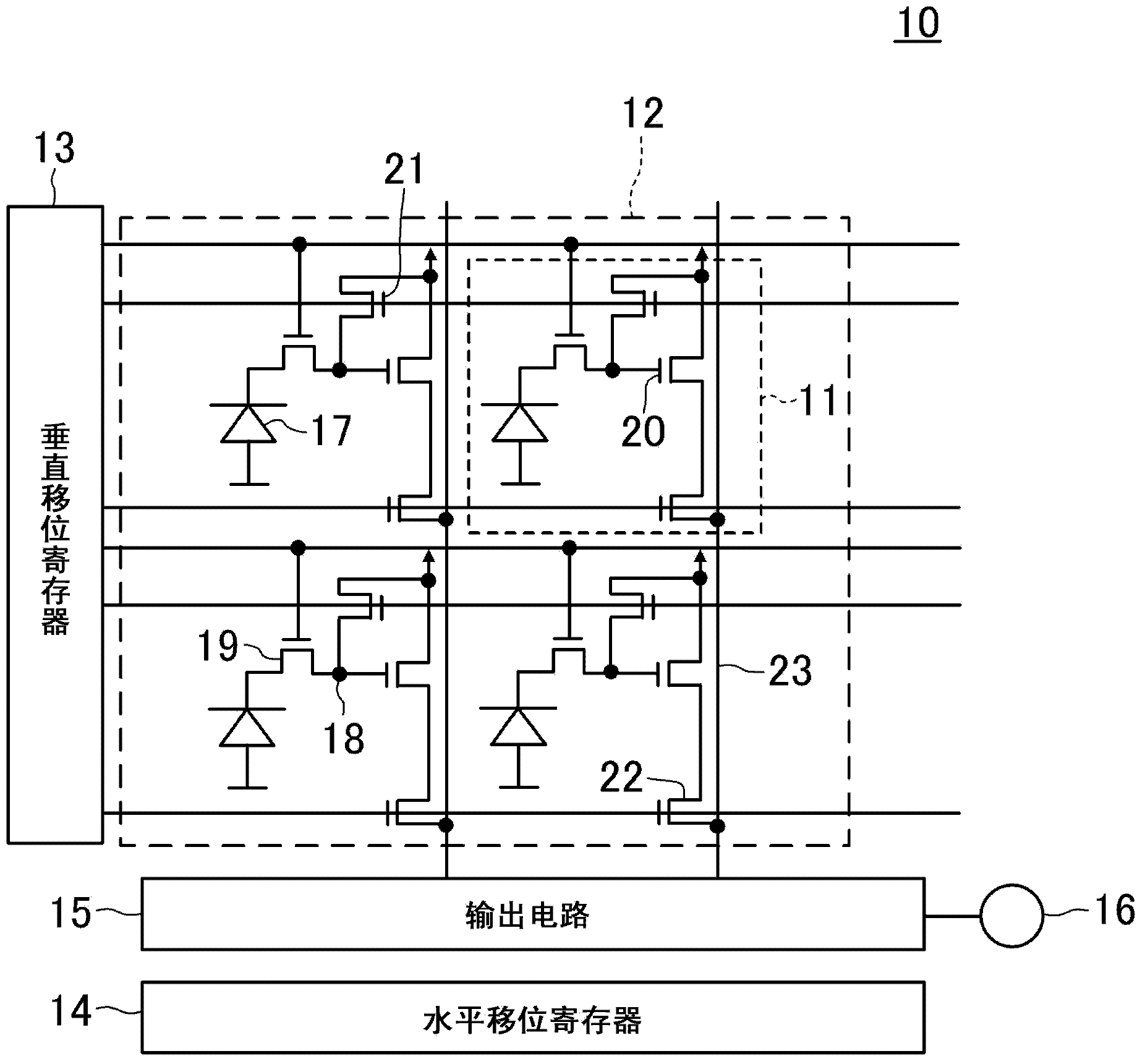
[0100] Such as figure 1 As shown, the solid-state imaging device 10 according to the first embodiment of the present invention is a MOS (Metal Oxide Semiconductor) image sensor (image sensor) in which a plurality of pixel units 11 are arranged in an array. The solid-state imaging device 10 has a pixel array region 12 including a plurality of pixel units 11 arranged in an array, a vertical shift register (shift register) 13 , a horizontal shift register 14 , an output circuit 15 , and an output terminal 16 .
[0101] The plurality of pixel units 1...
no. 2 Embodiment approach
[0119] refer to Figure 5 , the solid-state imaging device according to the second embodiment of the present invention will be described. In this embodiment, descriptions of the same configurations as those of the first embodiment are simplified or omitted, and only configurations different from those of the first embodiment will be described in detail.
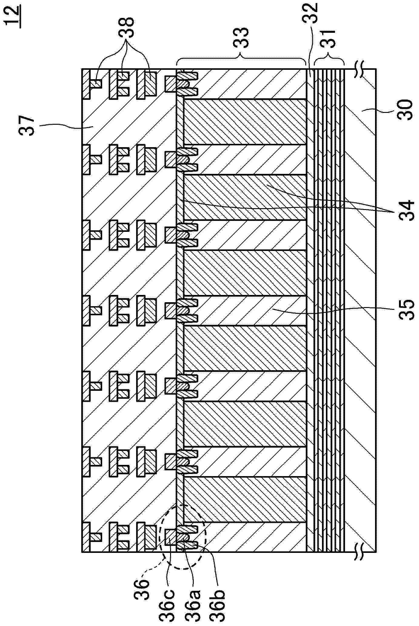
[0120] Such as Figure 5 As shown, in the pixel array region 12 , an imaging region 40 into which light enters and an optical black region 41 shielded from light so that light does not enter are provided. Further, between the imaging region 40 and the optical black region 41 , a groove portion 42 a penetrating the silicon layer 33 , the semiconductor layer 32 and the insulator layer 31 and exposing the surface of the semiconductor substrate 30 is formed. The groove portion 42a has a hollow structure, or is buried in a silicon oxide film, a polysilicon film, or the like.
[0121] In the imaging region 40 where light enters,...
no. 3 Embodiment approach
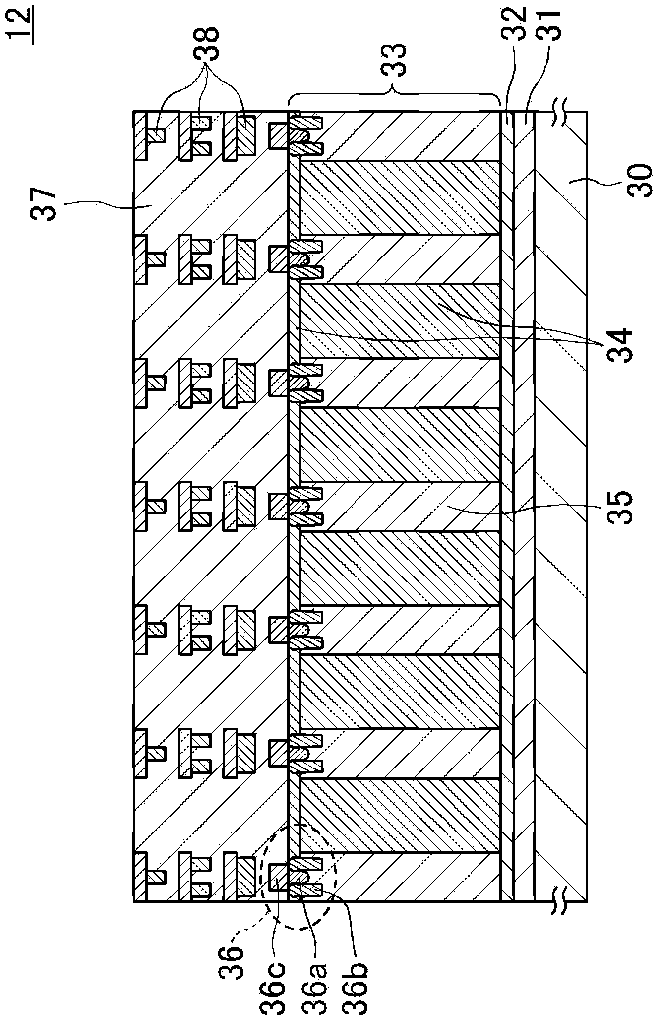
[0124] Next, refer to Figure 6 , the solid-state imaging device according to the third embodiment of the present invention will be described. In this embodiment, descriptions of the same configurations as those of the first embodiment are simplified or omitted, and only configurations different from those of the first embodiment will be described in detail.
[0125] Such as Figure 6 As shown, in the pixel array region 12, a plurality of photodiodes 34 are formed, and between adjacent photodiodes 34, a groove portion that penetrates the silicon layer 33, the semiconductor layer 32, and the insulator layer 31 and exposes the surface of the semiconductor substrate 30 is formed. 42b. The groove portion 42b has a hollow structure, or is buried in a silicon oxide film, a polysilicon film, or the like. Additionally, if Figure 6 As shown, the groove portion 42b is preferably formed at a position that does not affect the characteristics of the transfer transistor and the like. ...
PUM
 Abstract
Description
Claims
Application Information
 - R&D
- Intellectual Property
- Life Sciences
- Materials
- Tech Scout
- Unparalleled Data Quality
- Higher Quality Content
- 60% Fewer Hallucinations
Browse by: Latest US Patents, China's latest patents, Technical Efficacy Thesaurus, Application Domain, Technology Topic, Popular Technical Reports.
© 2025 PatSnap. All rights reserved.Legal|Privacy policy|Modern Slavery Act Transparency Statement|Sitemap|About US| Contact US: help@patsnap.com