


Quick Research
Generate reliable direction feasibility study reports for your R&D in just a few steps.

Technical Q&A
Discover and master advanced knowledge NOW. Basics, ideas, possibilities, all at once.

Find Solutions
As an expert in R&D theories, this can generate solutions to your technical problems instantly.

Evaluate Feasibility
Analyze your overall solution with one click, know your potential R&D risks in advance.

Monitor Landscape
Get weekly tech updates, stay abreast of the latest tech innovations and key insights.
Array substrate, liquid crystal display screen and display device
A liquid crystal display and array substrate technology, applied in nonlinear optics, instruments, optics, etc., can solve problems such as inability to realize double-sided display and normal viewing
- Summary
- Abstract
- Description
- Claims
- Application Information
AI Technical Summary
Problems solved by technology
Method used
Image


Examples
example 1
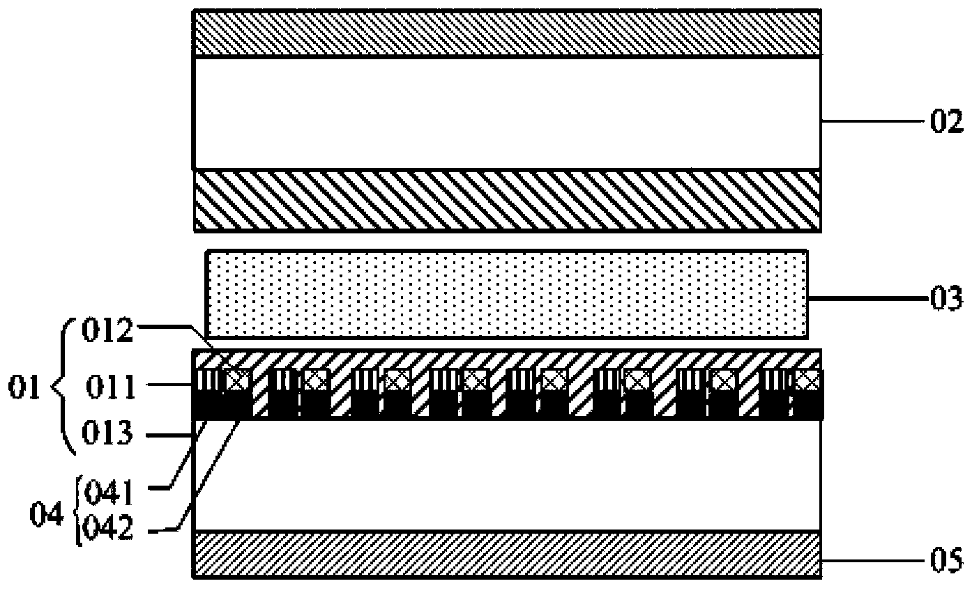
[0039] Such as Figure 2b As shown, the light blocking layer 04 can be disposed on the side of the base substrate 013 of the array substrate 01 facing the liquid crystal layer 03 , that is, the light blocking layer 04 is disposed between the base substrate 013 and the metal signal line 011 and the TFT device 012 .
example 2
[0041] The light blocking layer 04 may be located on a side of the base substrate 013 of the array substrate 01 away from the liquid crystal layer 03 . Specifically, as Figure 2c As shown, the light blocking layer 04 may be directly disposed on the side of the base substrate 013 away from the liquid crystal layer 03 .
example 3
[0043] The light blocking layer 04 may be located on a side of the base substrate 013 of the array substrate 01 away from the liquid crystal layer 03 . Specifically, as Figure 2d and Figure 2e As shown, a light-shielding substrate 06 may be disposed between the array substrate 01 and the polarizer 05 , and the light-shielding layer 04 may be disposed on the light-shielding substrate 06 . Specifically, as Figure 2d As shown, the light blocking layer 04 can be arranged on the side of the light blocking substrate 06 facing the array substrate 01; or, as Figure 2e As shown, the light blocking layer 04 may be disposed on the side of the light blocking substrate 06 away from the array substrate 01 . During specific implementation, the light blocking layer 04 may be fabricated on the light blocking substrate 06 first, and then the light blocking substrate 06 is attached to the array substrate 01 .
[0044] Based on the same inventive concept, an embodiment of the present inve...
PUM
 Abstract
Description
Claims
Application Information
 - R&D Engineer
- R&D Manager
- IP Professional
- Industry Leading Data Capabilities
- Powerful AI technology
- Patent DNA Extraction
Browse by: Latest US Patents, China's latest patents, Technical Efficacy Thesaurus, Application Domain, Technology Topic, Popular Technical Reports.
© 2024 PatSnap. All rights reserved.Legal|Privacy policy|Modern Slavery Act Transparency Statement|Sitemap|About US| Contact US: help@patsnap.com