Data automatic comparison test circuit of non-volatile memory

A test circuit, non-volatile technology, applied in the field of data automatic comparison test circuit, can solve the problems of address address dissatisfaction, not all 1, large circuit area, etc., to achieve the effect of flexible comparison, reduced use, and reduced implementation area

Active Publication Date: 2015-10-14
SHANGHAI HUAHONG GRACE SEMICON MFG CORP
View PDF2 Cites 0 Cited by
  • Summary
  • Abstract
  • Description
  • Claims
  • Application Information

AI Technical Summary

Problems solved by technology

Due to the different allocation of the row address (Ca), column address (Ra) and block address (Ba) of different types of non-volatile memory, that is, the addresses of Ca, Ra, and Ba of different series of non-volatile memory have certain differences , in the existing BIST circuit, an adder is generally set for each non-volatile memory to realize the accumulation of the address of each non-volatile memory, which will cause N adders to be generated in the BIST circuit to complete Automatic data comparison in N different ways, large circuit area
[0003] Although the same series of non-volatile memories have the same division of Ca, Ra, and Ba, due to the different capacities of each non-volatile memory such as Flash, the address may not be full (that is, not all 1).
In the existing BIST circuit, the maximum block address boundary is set, and the address returns when the block boundary is reached, but this method still cannot solve the situation that the column address is not full, and the address comparison needs to wait until the maximum address is compared before stopping, and the data Low flexibility for automatic comparison
[0004] The data automatic comparison circuit in the existing BIST circuit only supports fixed bit width comparison of data, that is, when the bit width of the output data is 32-bit, only 32-bit data comparison is performed, and the bit width of comparison cannot be flexibly controlled

Method used


Image

  • Data automatic comparison test circuit of non-volatile memory
  • Data automatic comparison test circuit of non-volatile memory
  • Data automatic comparison test circuit of non-volatile memory

Examples


Embodiment Construction

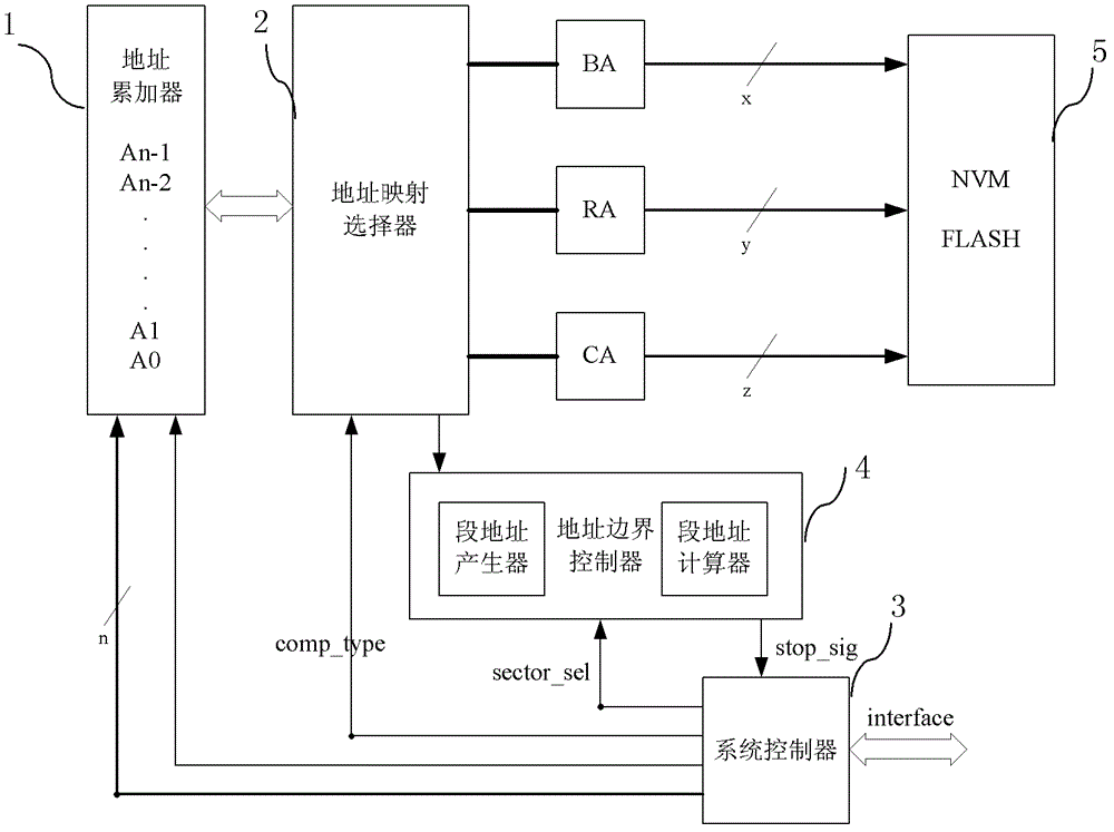
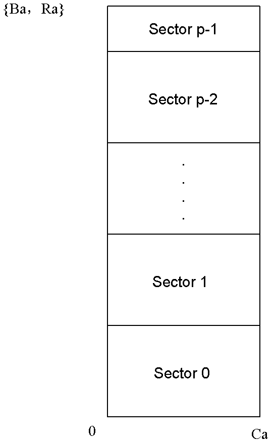
[0024] Such as figure 1 Shown is a circuit structure diagram of an embodiment of the present invention. The data automatic comparison test circuit of the non-volatile memory in the embodiment of the present invention includes: address accumulator 1, address mapping selector 2, system controller 3, address boundary controller 4 , Used for automatic data comparison test of non-volatile memory (NVM FLASH) 5. The non-volatile memory 5 includes a z-bit row address (Ca), a y-bit column address (Ra), and an x-bit block address (Ba).

[0025] The system controller 3 provides control signals for the address accumulator 1, the address mapping selector 2 and the address boundary controller 4. The system controller 3 is connected to an external testing machine through an interface.

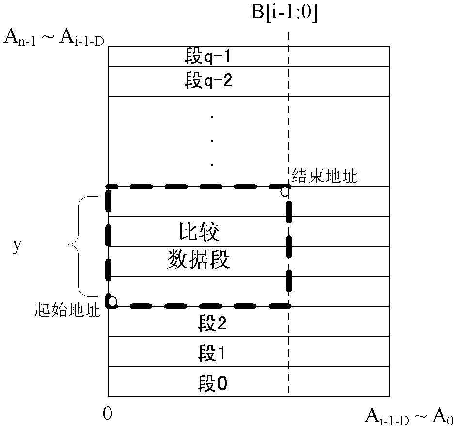
[0026] The address accumulator 1 is composed of n-bit address registers, and is used to add and subtract the test circuit addresses of the automatic data comparison test circuit. The n-bit test circuit addresses...


PUM


Abstract

The invention discloses a data automatically-comparing test circuit of a non-volatile memory, comprises an address accumulator, an address mapping selector, a system controller and an address boundary controller. The address accumulator is used for completing addition and subtraction of the test circuit. The address mapping selector is used for implementing mapping between a test circuit address and a non-volatile memory address, and for generating the non-volatile memory address. The address boundary controller is composed of a segment address generation module and a segment address calculation module, and is used for dividing the non-volatile memory into a plurality of data segments, calculating address boundary of each data segment, and generating a stop condition of segment comparison. The data automatically-comparing test circuit of a non-volatile memory can reduce usage of addition, can reduce a circuit area, can flexibly and effectively implement the segment comparison of the address, and can implement flexible comparison data with different bits.

Description

Technical field [0001] The invention relates to a semiconductor integrated circuit, in particular to a data automatic comparison test circuit of a non-volatile memory. Background technique [0002] In the prior art, non-volatile memory (NVM) generally requires a built-in self-test circuit (BIST) to pass the test. Because the row address (Ca), column address (Ra) and block address (Ba) of different types of non-volatile memory are allocated differently, the Ca, Ra, Ba addresses of different series of non-volatile memory have certain differences. In the existing BIST circuit, an adder is generally provided for each non-volatile memory to realize the accumulation of the address of each non-volatile memory. This will cause N adders to be generated in the BIST circuit to complete Automatic data comparison in N different ways, large circuit area. [0003] Although the non-volatile memories of the same series have the same divisions of Ca, Ra, and Ba, due to the different capacities of ...

Claims


Application Information

Patent Timeline
Patent Type & Authority Patents(China)
IPC IPC(8): G11C29/12
Inventor 高璐赵锋雷冬梅
Owner SHANGHAI HUAHONG GRACE SEMICON MFG CORP
Why Eureka
Try Eureka