CF (Colour Film) baseplate with touch function and touch panel
A technology of touch function and touch panel, which is applied in the input/output process of data processing, instruments, calculations, etc. It can solve the problems of broken glue width, thickness, and influence on conductivity, so as to achieve the goal of not easy to break glue, reduce spacing, and the effect of improving electrical conductivity
- Summary
- Abstract
- Description
- Claims
- Application Information
AI Technical Summary
Problems solved by technology
Method used
Image


Examples
Embodiment 1
[0062] In order to clearly understand the technical solution of the present invention, firstly, the method for fabricating the CF substrate provided in the first embodiment is introduced.
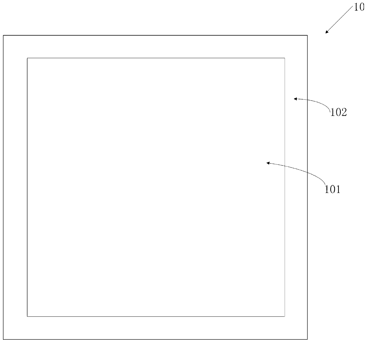
[0063] First, step S11 is performed to provide a substrate 10 .
[0064] Such as figure 1 As shown, the substrate 10 includes a display area 101 and a sealant coating area 102 disposed around the display area 101 . The substrate 10 is made of a transparent material, such as glass.
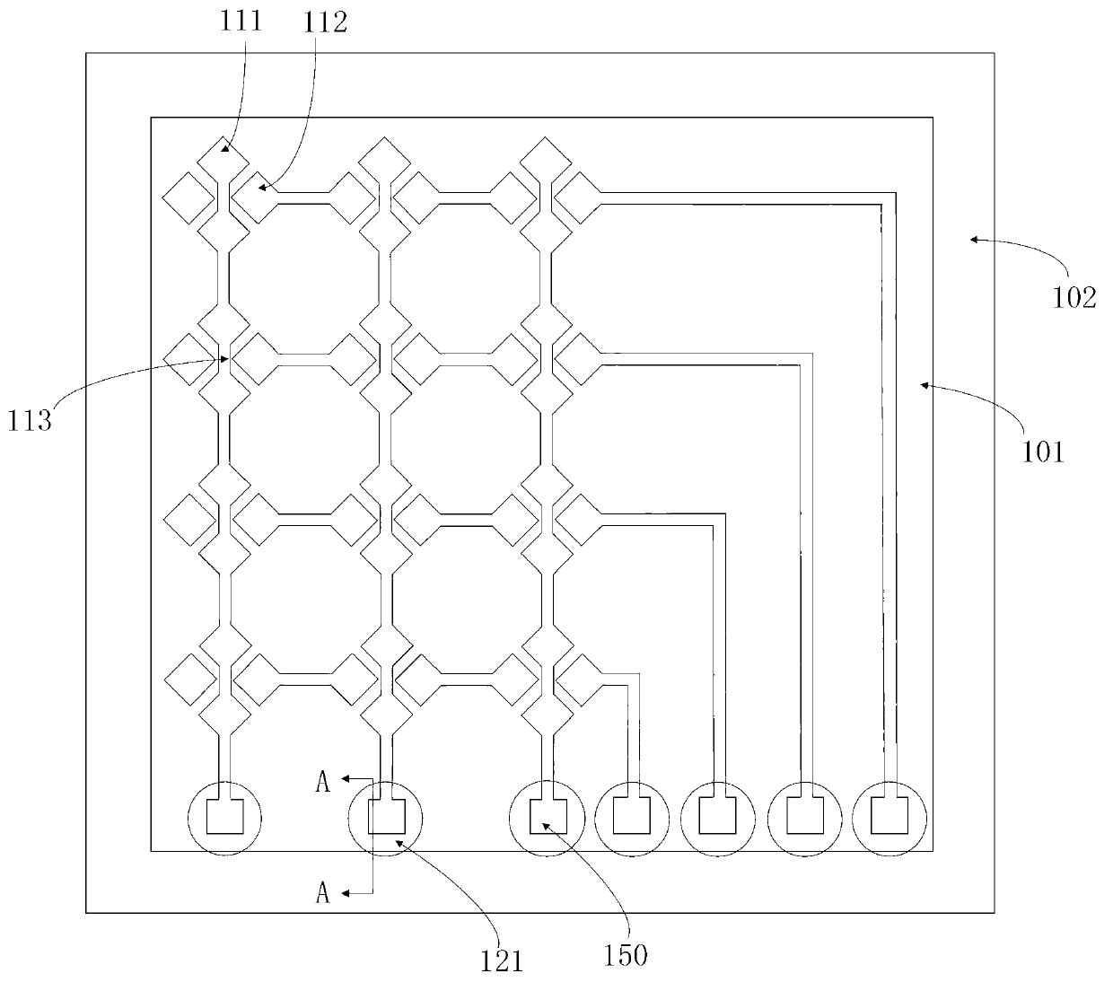
[0065] Next, execute step S12, refer to figure 2 As shown, a first conductive layer is deposited on the substrate 10, and etched to form a plurality of driving electrodes 111 and a plurality of sensing electrodes 112, as well as a plurality of first connecting lines 113, and a plurality of first connecting lines 113 connect a plurality of driving The electrodes 111 are connected together to form a driving line, and also form the first ends 150 of a plurality of first pins 2, the first ends 150 of the first ...
Embodiment 2
[0087] The structure and manufacturing method of the CF substrate provided in the second embodiment and the touch panel including the CF substrate are as follows:
[0088] Firstly, step S11 is performed to provide a substrate, which includes a display area 101 and a sealant coating area 102 arranged around the display area 101 .
[0089] Executing step S12, depositing a first conductive layer on the display area 101 of the substrate, and etching to form a plurality of driving electrodes 111, a plurality of sensing electrodes 112, and a plurality of first connection lines 113, the plurality of first connection lines 113 will A plurality of driving electrodes 111 are connected together to form a driving line, and simultaneously form a plurality of first ends 150 of the first pins 2, and the first ends 150 of the plurality of first pins 2 are respectively connected to the driving electrodes 111 or sensing The electrodes 112 are connected. In the second embodiment, if Figure 10...
Embodiment 3
[0094] Unlike the above two schemes, such as Figure 15 As shown, part of the first end 150 of the first pin in step S12 of the third embodiment is located in the display area 101 , and part is located in the sealant coating area 102 . Correspondingly, the cross-sectional structure of the formed touch panel (TFT substrate not shown) is as follows Figure 16 shown. In addition, the structure and manufacturing method of the CF substrate provided in the third embodiment and the touch panel including the CF substrate are the same as those in the first and second embodiments.
PUM
 Abstract
Description
Claims
Application Information
 - R&D
- Intellectual Property
- Life Sciences
- Materials
- Tech Scout
- Unparalleled Data Quality
- Higher Quality Content
- 60% Fewer Hallucinations
Browse by: Latest US Patents, China's latest patents, Technical Efficacy Thesaurus, Application Domain, Technology Topic, Popular Technical Reports.
© 2025 PatSnap. All rights reserved.Legal|Privacy policy|Modern Slavery Act Transparency Statement|Sitemap|About US| Contact US: help@patsnap.com