Prevention of light leakage in backside illuminated imaging sensors

A backside illumination and sensor device technology, which is applied in the field of backside illumination complementary metal oxide semiconductor imaging sensors, can solve problems such as interfering with the normal operation of BSI imaging sensors

Inactive Publication Date: 2013-08-14
OMNIVISION TECH INC
View PDF5 Cites 2 Cited by
  • Summary
  • Abstract
  • Description
  • Claims
  • Application Information

AI Technical Summary

Problems solved by technology

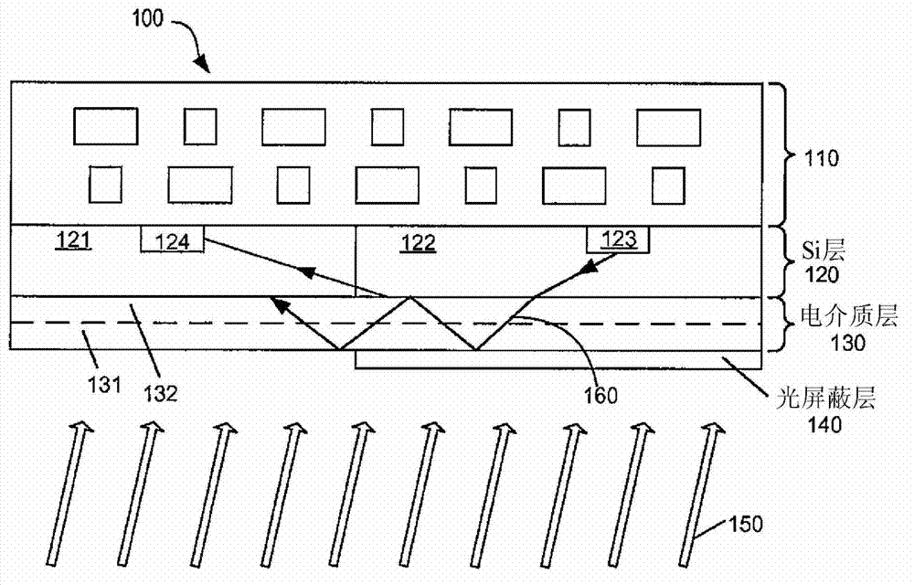
This lateral light can generate undesirable signals and interfere with the normal operation of BSI imaging sensors

Method used


Image

  • Prevention of light leakage in backside illuminated imaging sensors
  • Prevention of light leakage in backside illuminated imaging sensors
  • Prevention of light leakage in backside illuminated imaging sensors

Examples


Embodiment Construction

[0016] Embodiments of apparatus and methods for fabricating BSI imaging sensors that prevent light leakage are described herein. In the following description, numerous specific details are set forth in order to provide a thorough understanding of the embodiments. One skilled in the relevant art will recognize, however, that the techniques described herein may be practiced without one or more of the specific details or with other methods, components, materials, etc. In other instances, well-known structures, materials, or operations are not shown or described in detail to avoid obscuring the particular aspect.

[0017] Reference throughout this specification to "one embodiment" or "an embodiment" means that a particular feature, structure, or characteristic described in connection with the embodiment is included in at least one embodiment of the present invention. Thus, appearances of "in one embodiment" or "in an embodiment" in various places throughout this specification are...


PUM


Abstract

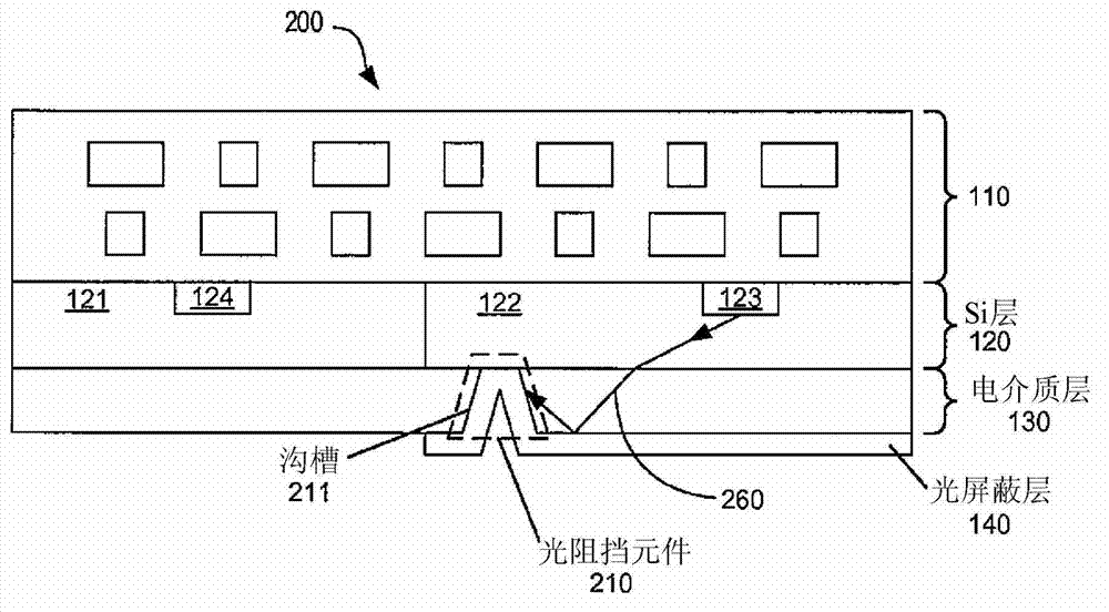
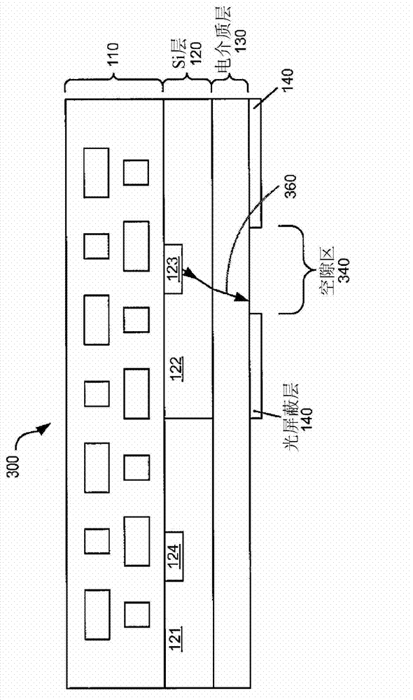
An apparatus includes a semiconductor layer, a dielectric layer, and a light prevention structure. The semiconductor layer has a front surface and a backside surface. The semiconductor layer includes a light sensing element and a periphery circuit region containing a light emitting element and not containing the light sensing element. The dielectric layer contacts at least a portion of the backside surface of the semiconductor layer. At least a portion of the light prevention structure is disposed between the light sensing element and the light emitting element. The light prevention structure is positioned to prevent light emitted by the light emitting element from reaching the light sensing element.

Description

technical field [0001] The present invention relates generally to imaging sensors, and in particular, but not exclusively, to backside illuminated ("BSI") complementary metal-oxide-semiconductor ("CMOS") imaging sensors. Background technique [0002] Many semiconductor imaging sensors today are frontside illuminated. That is, these sensors comprise an imaging array fabricated on the front side of a semiconductor wafer, where incoming light is received at the imaging array from the same front side. Front side illuminated imaging sensors have several disadvantages such as limited fill factor. [0003] BSI imaging sensors are an alternative to front side illuminated imaging sensors. BSI imaging sensors comprise an imaging array fabricated on the front surface of a semiconductor wafer, but receive incoming light via the back surface of the wafer. At the back surface, a portion of the incoming light enters the device wafer, while another portion of the incoming light is reflec...

Claims


Application Information

Patent Timeline
Patent Type & Authority Applications(China)
IPC IPC(8): H01L27/146
CPCH01L27/14623H01L27/146H01L27/1464
Inventor 郑伟文森特 瓦乃兹艾戴幸志
Owner OMNIVISION TECH INC
Why Eureka
Try Eureka