Switching circuit

A technology of switching circuits and switching circuits, which is applied in the fields of electrical digital data processing, instruments, and detection of faulty computer hardware, etc.

Inactive Publication Date: 2013-07-03
国网山东省电力公司单县供电公司
View PDF2 Cites 9 Cited by
  • Summary
  • Abstract
  • Description
  • Claims
  • Application Information

AI Technical Summary

Problems solved by technology

However, when the motherboard is debugged and the BIOS chip supporting the SPI interface is set on the motherboard, the resistance values ​​of the resistors R1-R4 need to be replaced (for example, the resistance value of the resistor R2 is set to be extremely small relative to the resistance value of the resistor R1 1. Set the resistance value of resistor R4 to be extremely small relative to the resistance value of resistor R3), so that the two trigger pins of PCH chip 10 receive a low level, and then select a BIOS chip that supports the SPI interface to start the mainboard, so that Great inconvenience to developers

Method used


Image

  • Switching circuit
  • Switching circuit
  • Switching circuit

Examples


Embodiment Construction

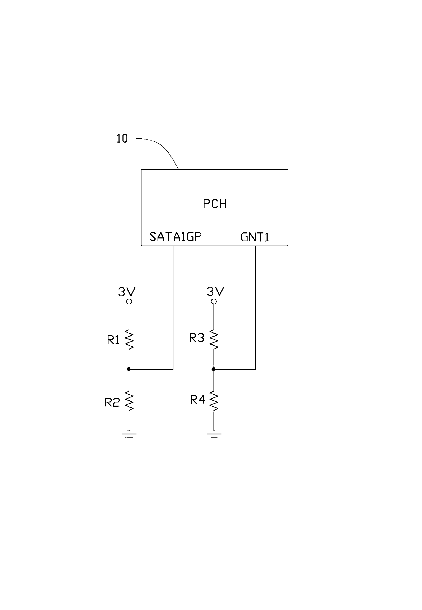
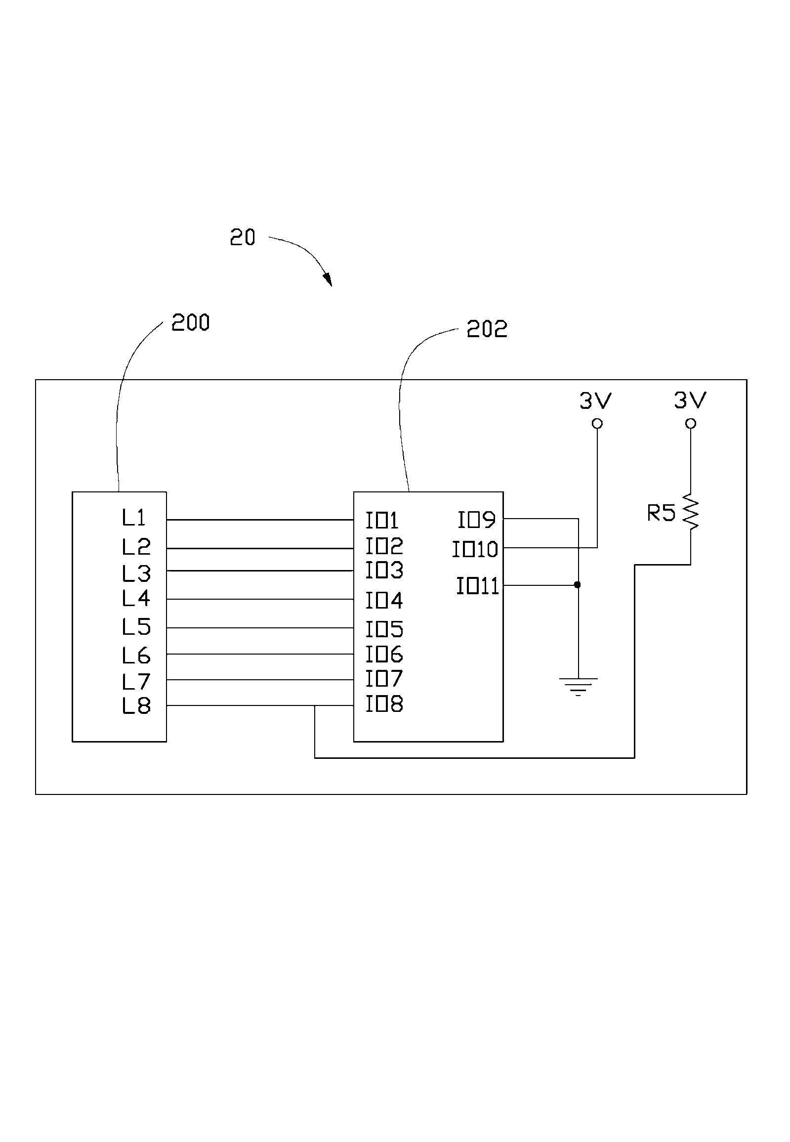
[0023] Please refer to Figure 2 to Figure 4 The preferred embodiment of the switching circuit of the present invention includes a diagnostic card 20, a first connector 300, a PCH chip 301, a first BIOS chip 302, and a switch circuit 303. The first connector 300, the PCH chip 301, the first BIOS chip 302 and the switch circuit 303 are all arranged on a motherboard 30.

[0024] The diagnostic card 20 includes a second connector 200, a second BIOS chip 202, and a resistor R5. When debugging the motherboard 30, the second BIOS chip 202 is used to start the motherboard 30. The second connector 200 is connected to the second BIOS chip 202 through the LPC bus. The pin IO1 of the second BIOS chip 202 is used to transmit a clock signal to the pin L1 of the second connector 200, and the pin IO2 is used to transmit a reset signal to the pin L2 and the pin IO3 of the second connector 200 -IO6 is used to transmit address signals to the pins L3-L6 of the second connector 200, and the pin I...


PUM


Abstract

The invention discloses a switching circuit, which comprises a first connector, a first platform controller hub (PCH), a first basic input output system (BIOS), a diagnosis card and a switch circuit. The PCH comprises a first strapping pin and a second strapping pin. The diagnosis card comprises a second connector and a second BIOS. The second connector is plugged into the first connector. The second BIOS is used for outputting a high-potential control signal. The switch circuit is used for receiving the control signal sent from the second BIOS. When the switch circuit receives the high-potential control signal, the switch circuit outputs a high-potential switch signal to the first and second strapping pins of the PCH. When the switch circuit does not receive the high-potential control signal, the switch circuit outputs a low-potential switch signal to the first and second strapping pins. The switching circuit can be used for conveniently switching the first or second BIOS to start a main board, thereby bringing convenience to research personnel.

Description

Technical field [0001] The invention relates to a switching circuit, in particular to a switching circuit that simulates a motherboard BIOS chip through a diagnostic card. Background technique [0002] The BIOS (Basic Input Output System) chips set on the existing motherboards exchange data with PCH (Platform Controller Hub) chips through SPI (Serial Peripheral Interface) bus. . In the motherboard design and development stage, a Debug Card is usually used to simulate the BIOS chip on the motherboard. This diagnostic card exchanges data with the PCH chip through the LPC (Low Pin Count) bus. This diagnostic card can display the status information of each hardware of the motherboard when it is turned on. Therefore, the research and development personnel can judge the working status of each hardware based on the displayed information. [0003] Please refer to figure 1 The PCH chip 10 includes two strapping pins SATA1GP and GNT1. One end of the resistor R1 is connected to the power s...

Claims


Application Information

Patent Timeline
Patent Type & Authority Applications(China)
IPC IPC(8): G06F11/22
CPCG06F13/4022
Inventor 邹华陈俊生
Owner 国网山东省电力公司单县供电公司
Why Eureka
Try Eureka