Insulated gate bipolar transistor device structure and fabrication method thereof

A technology of bipolar transistors and device structures, which is applied in semiconductor/solid-state device manufacturing, semiconductor devices, electrical components, etc., and can solve problems such as large turn-off loss and long device turn-off time.

Active Publication Date: 2016-10-26
SHANGHAI HUAHONG GRACE SEMICON MFG CORP
View PDF3 Cites 0 Cited by
  • Summary
  • Abstract
  • Description
  • Claims
  • Application Information

AI Technical Summary

Problems solved by technology

[0002] IGBT is a high-power discrete device with high withstand voltage and conductivity. Its disadvantage is that when the device is turned off, there will be a large tail current, and the tail current will gradually decrease, resulting in the off-time of the device. longer, and produces larger turn-off losses

Method used


Image

  • Insulated gate bipolar transistor device structure and fabrication method thereof
  • Insulated gate bipolar transistor device structure and fabrication method thereof
  • Insulated gate bipolar transistor device structure and fabrication method thereof

Examples


Embodiment 1

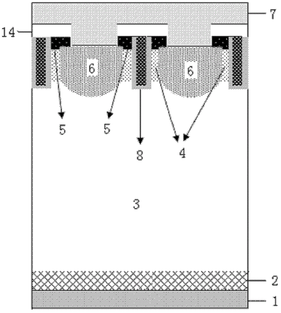
[0024] Embodiment one, see Figure 3-5 shown.

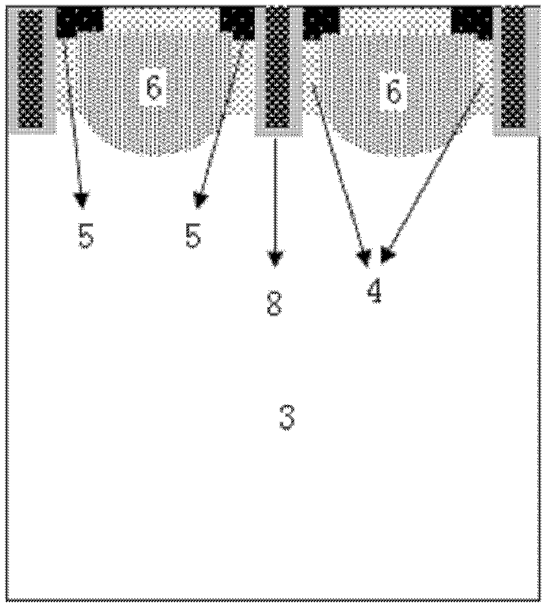
[0025] Step 1. Combine image 3 As shown, an N-type voltage-resistant body region 3 is formed, and a P body region 6 , a channel region 4 , a trench 8 and an N+ emitter region 5 are respectively formed on the upper end of the N-type voltage-resistant body region 3 . That is to complete the manufacturing process of the main structure on the front of the device, which can be completed by using various existing manufacturing process methods.

[0026] Step two, combine Figure 4 As shown, a plurality of deep trenches are etched at the lower end of the N-type voltage-resistant body region, and a super junction structure region 9 is formed by using an existing super junction structure manufacturing method. For example, the super junction structure region 9 composed of alternately arranged N-type semiconductors and P-type semiconductors is formed by filling the trenches with epitaxial growth.

[0027] Step three, combine Figure 5 ...

Embodiment 2

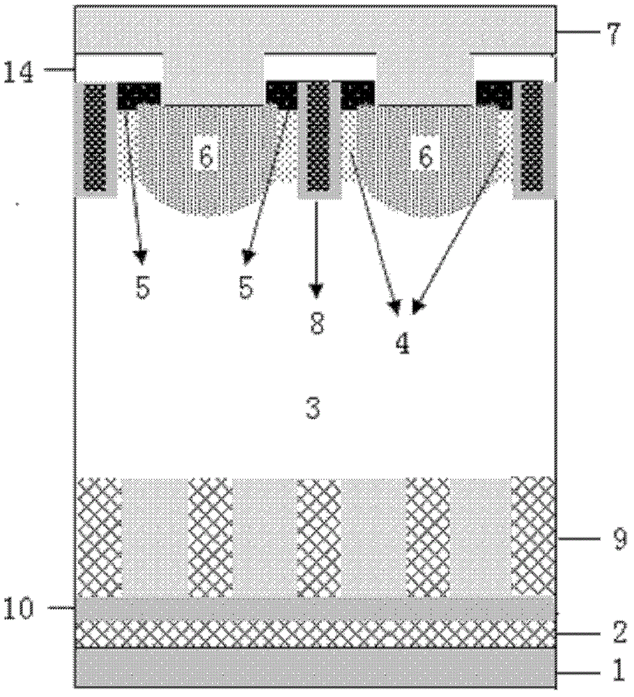
[0030] Embodiment two, combining Figure 6-8 shown.

[0031] Step 1. Combine Figure 6 As shown, the super junction structure region 9 is formed on the upper end of the higher concentration N-type substrate 11 .

[0032] Step 2. Combine Figure 7 As shown, an N-type voltage-resistant body region 3 with a lower concentration and a certain thickness is epitaxially grown on the upper end of the super junction structure region 9 . The thickness of the N-type withstand voltage body region 3 is determined by the withstand voltage level of the device.

[0033] Step 3. Combine Figure 8 As shown, the front structure of the device is formed on the upper end of the N-type voltage-resistant body region (the front side of the device), that is, the P body region 6, the channel region 4, the trench 8, the N+ emitter region 8 and the isolation dielectric layer 14 are formed respectively; After metallization, the emitter 7 is formed.

[0034] Step 4. Combine figure 2 , 8 As shown, th...


PUM


Abstract

The invention discloses an insulated gate bipolar transistor device structure which comprises an N type withstand voltage body region, a P body region located at the upper end of the N type withstand voltage body region, a channel region formed on two sides of the P body region, an N+ transmission region located at the upper ends of the channel region and the P body region, a groove formed at the lateral ends of the N+ transmission region and the channel region, an isolation medium layer located at the upper ends of the groove and the N+ transmission region and an emitter located at the upper end of the isolation medium layer and led out from the P body region. A super junction structure region, an N type region, a P+ collector region and a collector are sequentially formed at the lower end of the N type withstand voltage body region. A manufacture method of the insulated gate bipolar transistor device structure is further disclosed. The structure and the method can effectively reduce turn-off loss of devices.

Description

technical field [0001] The invention relates to the field of semiconductor integrated circuits, in particular to an insulated gate bipolar transistor (IGBT) device structure. The invention also relates to a method of fabricating said transistor device structure. Background technique [0002] IGBT is a high-power discrete device with high withstand voltage and conductivity. Its disadvantage is that when the device is turned off, there will be a large tail current, and the tail current will gradually decrease, resulting in the off-time of the device. It is longer and produces a large turn-off loss. The trailing current has a lot to do with the PN junction formed at the back collector terminal. Compared with IGBT, the high-power discrete device with super junction structure has a small tail current although its withstand voltage and conductivity are slightly lower. Contents of the invention [0003] The technical problem to be solved by the present invention is to provide ...

Claims


Application Information

Patent Timeline
Patent Type & Authority Patents(China)
IPC IPC(8): H01L29/739H01L29/06H01L21/331
Inventor 张帅刘坤
Owner SHANGHAI HUAHONG GRACE SEMICON MFG CORP
Why Eureka
Try Eureka