Patch type diode device structure

A device structure and diode technology, applied in the direction of electrical solid-state devices, semiconductor devices, semiconductor/solid-state device components, etc., can solve problems such as product electrical or reliability failures, avoid product yield loss, and improve product electrical properties and reliability, avoiding the effect of connecting piece deviation

Active Publication Date: 2013-05-22
SUZHOU GOODARK ELECTRONICS CO LTD
View PDF3 Cites 12 Cited by
  • Summary
  • Abstract
  • Description
  • Claims
  • Application Information

AI Technical Summary

Problems solved by technology

During the molding process, injection molding pores are prone to appear inside the product. These pores can lead to electrical or reliability failure of the product. Therefore, how to develop a semiconductor packaging structure that is easy to locate and can solve the above problems has become the direction of efforts of those skilled in the art.

Method used


Image

  • Patch type diode device structure
  • Patch type diode device structure
  • Patch type diode device structure

Examples


Embodiment

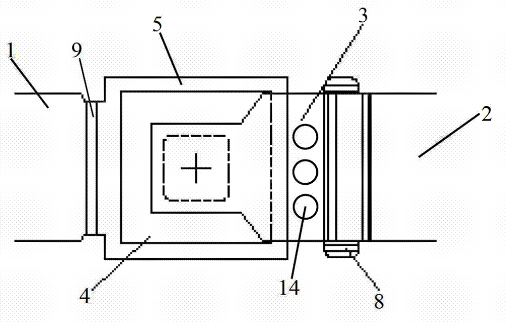
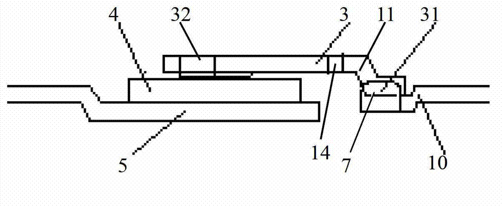
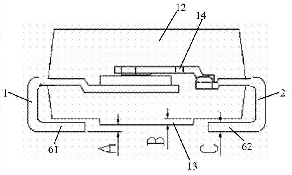
[0025] Example: a chip diode device structure, as attached Figures 1~3 As shown, it includes a first lead bar 1, a second lead bar 2, a connecting piece 3 and a diode chip 4 located in the epoxy package 12, and one end of the first lead bar 1 is a support area 5 connected to the diode chip 4, One end of the diode chip 4 is electrically connected to the support area 5 through solder paste, the other end of the first lead bar 1 is a pin area 61, and the pin area 61 of the first lead bar 1 serves as the current transmission end of the rectifier;

[0026] One end of the second lead bar 2 is a welding area 7 connected to the first welding end 31 of the connecting piece 3 , the other end of the second lead bar 2 is a pin area 62 , and the pins of the second lead bar 2 Region 62 serves as the current transfer terminal of the rectifier;

[0027] The second welding end 32 of the connecting piece 3 is electrically connected with the other end of the diode chip 4 through solder paste; ...


PUM


Abstract

The invention relates to a patch type diode device structure. The patch type diode device structure comprises a first lead strip, a second lead strip, a connecting piece and a diode chip which are arranged in an epoxy packaging body, wherein a first bending position is arranged in an area between a support area of the first lead strip and a pin area, so that the support area of the first lead strip is lower than the pin area; a second bending position is arranged in an area between a welding area of the second lead strip and the pin area, so that the welding area of the second lead strip is lower than the pin area; a third bending position is arranged between a first welding end and a second welding end of the connecting piece, so that the first welding end is lower than the second welding end; a protrusion portion with thickness smaller than that of the pin area is arranged on the lower surface of the epoxy packaging body; and a plurality of through holes are arranged between the third bending position and the second welding end. The patch type diode device structure eliminates the possibility that a pin suspension degree is below a lower limit, so that product yield loss caused by an ultra lower limit of a suspension degree value in case of unit abnormality and product abnormality caused by miss-judging are avoided.

Description

technical field [0001] The invention relates to a diode device, in particular to a chip diode device structure. Background technique [0002] Rectifiers use the unidirectional conduction characteristics of diodes to rectify alternating current, so they are widely used in circuits that convert alternating current into direct current. [0003] Existing semiconductor products with connecting piece structure usually limit the connecting piece with no limit or adopt a simple groove structure. The disadvantage is that the connecting piece can only be limited in one direction. The purpose of the limit is to avoid the connection during the welding process in the furnace. Chip offset causes the connection points on the connecting chip to deviate from the chip bonding area, resulting in electrical failure of the product. When the device design requires a higher-precision limit for the connecting piece, the existing structure cannot meet the requirements. The purpose of the limit is t...

Claims


Application Information

Patent Timeline
Patent Type & Authority Applications(China)
IPC IPC(8): H01L33/62H01L33/54
CPCH01L23/3114H01L23/3121H01L24/40H01L23/481H01L2224/40245H01L2224/40091H01L2924/181H01L2224/4007H01L2224/37011H01L2224/84801H01L2924/00014H01L2224/84385H01L2224/40H01L24/84H01L2224/84345H01L2924/00012H01L2224/37099
Inventor 张雄杰何洪运程琳
Owner SUZHOU GOODARK ELECTRONICS CO LTD
Why Eureka
Try Eureka