Novel 3D optical stereoscopic diaphragm and production method thereof
A three-dimensional film and optical technology, applied in optics, optical components, instruments, etc., can solve the problems of reduced brightness, large flicker, and small visual depth, and achieve the effects of increasing brightness, reducing dosage, and reducing flicker
- Summary
- Abstract
- Description
- Claims
- Application Information
AI Technical Summary
Problems solved by technology
Method used
Image
Examples
Embodiment 1
[0026] like figure 1 As shown, first, a certain amount of polyethylene terephthalate (PET) material, containing appropriate heat-resistant stabilizers, is co-extruded on a co-extrusion casting extruder, and passed through 72 hours of static Afterwards, the finished products are cut into pieces, and the thickness of the transparent film material layer 1 is 0.01mm. Secondly, titanium dioxide nanoparticles were prepared by a sol-gel method, and titanium dioxide nanoparticles 3 with a size of 10 nm were doped in the electronic ink at a ratio of 10%. Finally, the electronic ink is prepared on the PET transparent film layer by an inkjet printing method to form a uniformly arranged slit grating layer 2 .
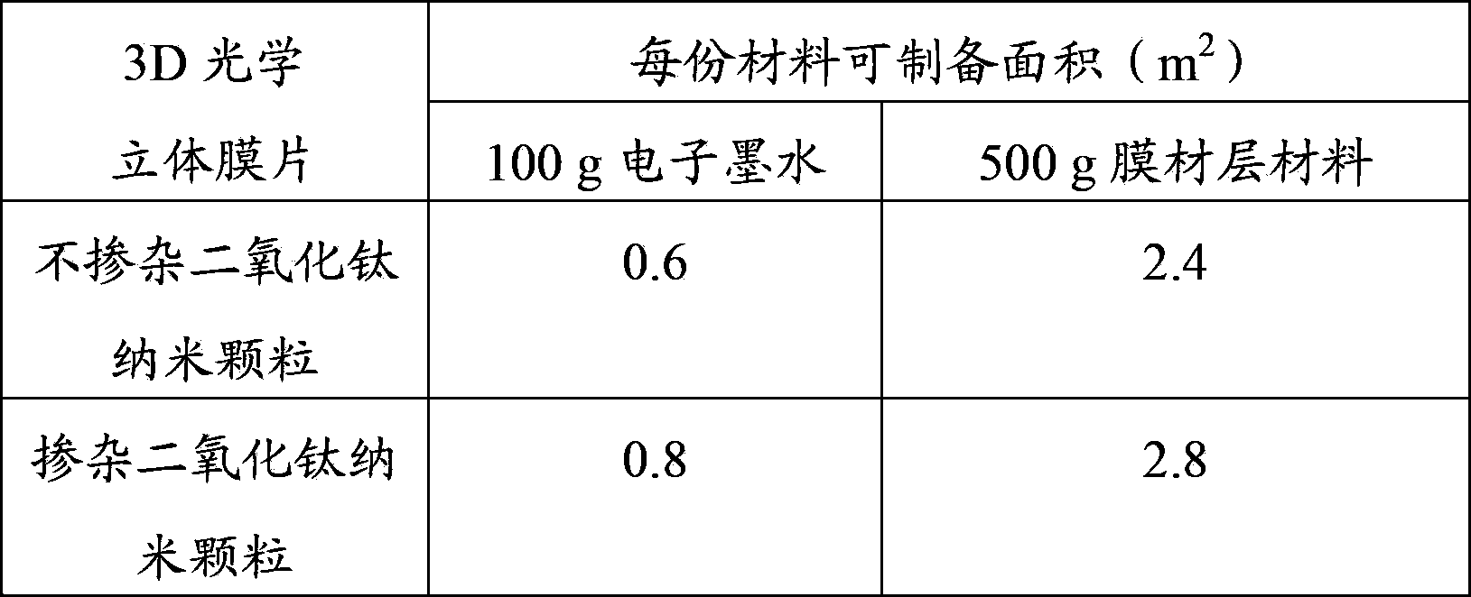
[0027] Table 1
[0028]
[0029] Table 1 is the cost comparison of the 3D optical three-dimensional film prepared without doping titanium dioxide nanoparticles and doping titanium dioxide nanoparticles in the electronic ink in Example 1.
[0030] Table 2
[0031] Vi...
Embodiment 2
[0035] like figure 1 As shown, first, a certain amount of polyethylene (PE) material, containing a suitable heat-resistant stabilizer, is co-extruded on a co-extrusion casting extruder, and then cut into pieces after 72 hours of static product, the thickness of the transparent film material layer 1 is 2mm. Secondly, titanium dioxide nanoparticles were prepared by thermal synthesis, and titanium dioxide nanoparticles 3 with a size of 60 nm were doped in the electronic ink at a ratio of 2%. Finally, the electronic ink is prepared on the PE transparent film material layer by a spraying method to form a uniformly arranged slit grating strip layer 2 .
Embodiment 3
[0037] like figure 1 As shown, first, a certain amount of polyethylene naphthalate (PEN) material, containing appropriate heat-resistant stabilizers, is co-extruded on a co-extrusion casting extruder, and passed through 72 hours of static Slitting into finished products is carried out again, and the thickness of the transparent film material layer 1 is 1mm. Secondly, titanium dioxide nanoparticles were prepared by alkoxide hydrolysis, and titanium dioxide nanoparticles 3 with a size of 100 nm were doped in the electronic ink at a ratio of 0.1%. Finally, the electronic ink is prepared on the PEN transparent film material layer by an inkjet printing method to form a uniformly arranged slit grating layer 2 .
PUM
 Abstract
Description
Claims
Application Information
 - R&D Engineer
- R&D Manager
- IP Professional
- Industry Leading Data Capabilities
- Powerful AI technology
- Patent DNA Extraction
Browse by: Latest US Patents, China's latest patents, Technical Efficacy Thesaurus, Application Domain, Technology Topic, Popular Technical Reports.
© 2024 PatSnap. All rights reserved.Legal|Privacy policy|Modern Slavery Act Transparency Statement|Sitemap|About US| Contact US: help@patsnap.com


