
Active power factor correction circuit

A technology for calibrating circuits and source power, applied in output power conversion devices, electrical components, energy industries, etc. Responsive, reduced size effects

Active Publication Date: 2015-04-08
XIDIAN UNIV
View PDF5 Cites 0 Cited by
  • Summary
  • Abstract
  • Description
  • Claims
  • Application Information

AI Technical Summary

Problems solved by technology

Since the size of the external inductor used in the active power factor correction circuit is proportional to the output voltage V OUT with input voltage V in Therefore, the size of the peripheral inductance used in the existing active power factor correction circuit is very large, which increases the volume of electronic equipment and limits the development of electronic equipment in the direction of portable

Method used


Image

  • Active power factor correction circuit
  • Active power factor correction circuit
  • Active power factor correction circuit

Examples


Embodiment Construction

[0031] The present invention will be further described below with reference to the accompanying drawings and the embodiments thereof.

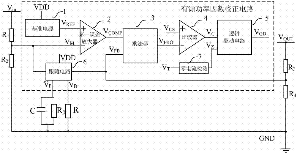
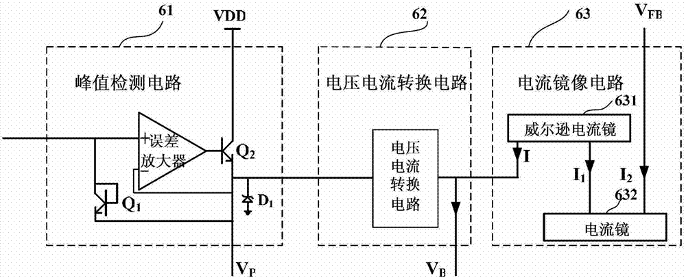
[0032] refer to figure 2 , the active power factor correction circuit of the present invention includes: a reference power supply 1, a first error amplifier 2, a multiplier 3, a comparator 4, a logic drive circuit 5, a follower circuit 6, and a zero current detection 7; the reference power supply 1 is used to generate Reference voltage V REF ; The reference voltage V REF connected to the first error amplifier 2, the first error amplifier 2 to the reference voltage V REF Compare and amplify with the input signal VM of the chip where it is located, and output the differential signal V COMP ; The differential signal V COMP connected to Multiplier 3, which converts the differential signal V COMP It is multiplied by the input signal VFB of the chip where it is located, and the output product signal V PRO ; Comparator 4 pairs product signal V...


PUM


Abstract

The invention discloses an active power factor correction circuit which mainly solves the problem that a peripheral inductor is large in size in the prior art. The circuit comprises a reference power supply (1), a first error amplifier (2), a multiplier (3), a comparator (4), a logic driving circuit (5), a follower circuit (6) and a zero current detector (7), wherein output reference voltage of the reference power supply (1) is connected with the first error amplifier (2); an output of the first error amplifier (2) is connected with the multiplier (3); an output of the multiplier (3) is connected with the comparator (4); an output (4) the comparator (4) and an output of the zero current detector (7) are connected with the logic driving circuit (5); the logic driving circuit (5) generates an output signal of a chip where the logic driving circuit (5) is located; the follower circuit (6) is in bridge connection between the first error amplifier (2) and the multiplier (3); current is extracted from an input end of the multiplier (3); and output voltage Vout varies with input voltage Vin. With the adoption of the active power factor correction circuit, the size of the peripheral inductor adopted by the active power factor correction circuit is reduced effectively, and the active power factor correction circuit can be applied to electronic equipment adopting the active power factor correction circuit.

Description

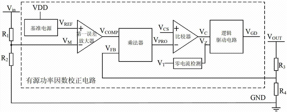
technical field [0001] The invention belongs to the technical field of electronic circuits, and relates to an analog integrated circuit, in particular to an active power factor correction circuit. Background technique [0002] As a very important power management circuit, active power factor correction is widely used in various electronic devices. After the active power factor correction is applied to the rectification and filtering circuit, it usually provides a power factor value close to 1. Therefore, the active power factor correction circuit can reduce the harmonic pollution of the electronic equipment to the power grid and improve the utilization rate of electric energy. Compared with the commonly used passive power factor correction circuit, it has the advantages of high power factor value and small volume. [0003] The structure of the existing active power factor correction circuit is as follows figure 1 As shown, the active power factor correction circuit is comp...

Claims


Application Information

Patent Timeline
Patent Type & Authority Patents(China)
IPC IPC(8): H02M1/42
CPCY02B70/126Y02B70/10Y02P80/10
Inventor 来新泉袁冰关会丽赵永瑞
Owner XIDIAN UNIV
Learn More