Small ultra wideband band-notched antenna with controllable second-order notched bandwidth
A notch antenna and ultra-wideband technology, applied in the field of planar miniaturized ultra-wideband notch antenna, can solve the problems of large size of ultra-wideband antenna, uncontrollable notch bandwidth, poor selectivity, etc. Improved, selective effect
- Summary
- Abstract
- Description
- Claims
- Application Information
AI Technical Summary
Problems solved by technology
Method used
Image
Examples
Embodiment
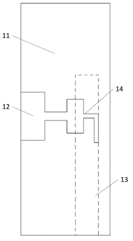
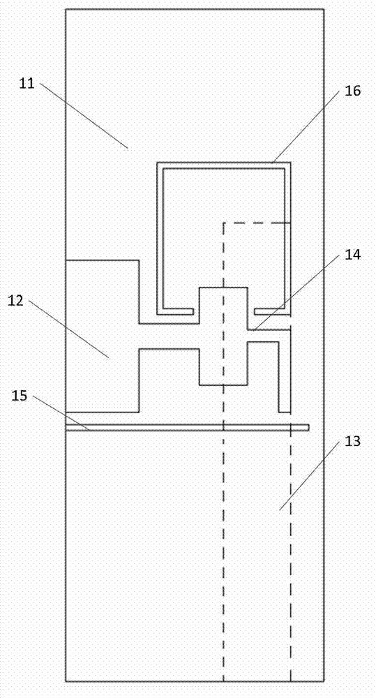
[0023] figure 1 It is the geometric structure of the small ultra-wideband antenna proposed by the present invention, which is printed on a dielectric board with a size of 22×8.5×0.8 mm, that is, on the FR4 substrate 12. The front side of the dielectric plate is a bent step width gap 14; the back side of the dielectric plate is a 50-ohm microstrip feeder line 13. The electromagnetic wave on the microstrip feeder 13 is coupled to the step width gap 14 and radiated. The step width slits 14 can form multiple matching points in the frequency range of the ultra-wideband. These matching points can be controlled by adjusting the size of the step width slits to make them uniformly distributed in the frequency range of the ultra-wideband. The relative position between the microstrip feed line 13 and the step width slot 14 also has an important influence on the impedance matching characteristics of the entire antenna. By adjusting these parameters with software, this antenna can achieve ...
PUM
 Abstract
Description
Claims
Application Information
 - R&D
- Intellectual Property
- Life Sciences
- Materials
- Tech Scout
- Unparalleled Data Quality
- Higher Quality Content
- 60% Fewer Hallucinations
Browse by: Latest US Patents, China's latest patents, Technical Efficacy Thesaurus, Application Domain, Technology Topic, Popular Technical Reports.
© 2025 PatSnap. All rights reserved.Legal|Privacy policy|Modern Slavery Act Transparency Statement|Sitemap|About US| Contact US: help@patsnap.com


