Optoelectronic device and method for manufacturing an optoelectronic device
一种光电子器件、发光材料的技术,应用在发光装置,制造光电子器件领域,能够解决颗粒密度的梯度耗费、难以复现、昂贵等问题,达到高光学效率、均匀光密度的效果
- Summary
- Abstract
- Description
- Claims
- Application Information
AI Technical Summary
Problems solved by technology
Method used
Image

Examples
Embodiment Construction
[0054] Elements that are the same, of the same kind or have the same function are provided with the same reference signs in the drawings. The drawings and the size ratios of the elements shown in the drawings to each other cannot be shown to be to scale. On the contrary, for better description and for better understanding, various elements can be shown exaggerated.
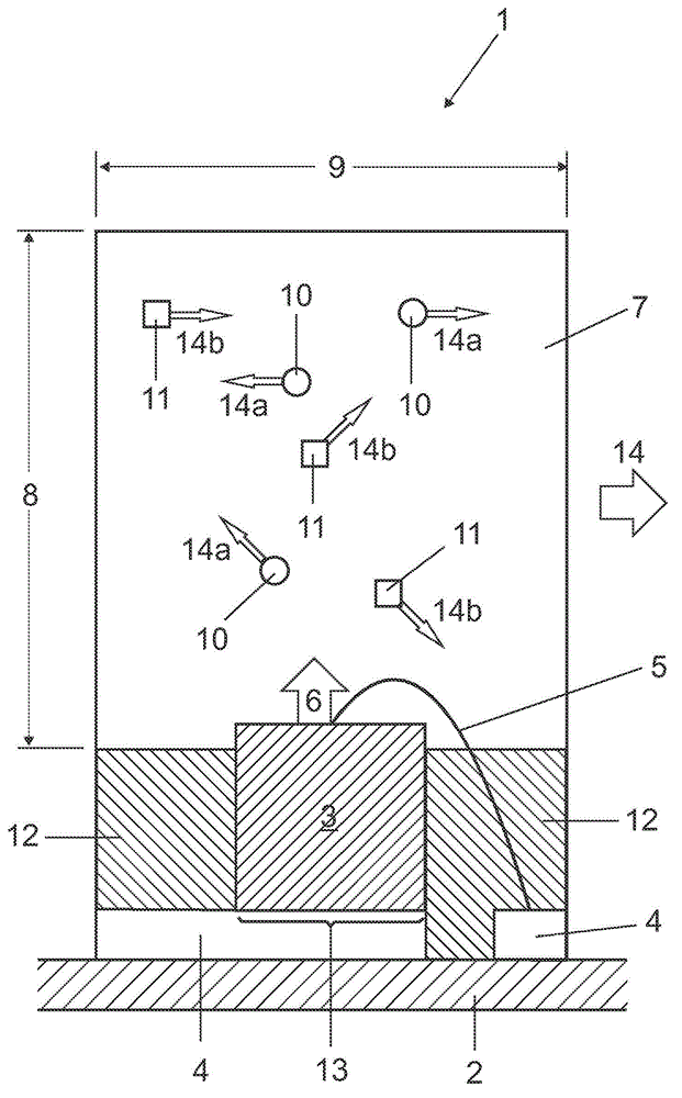
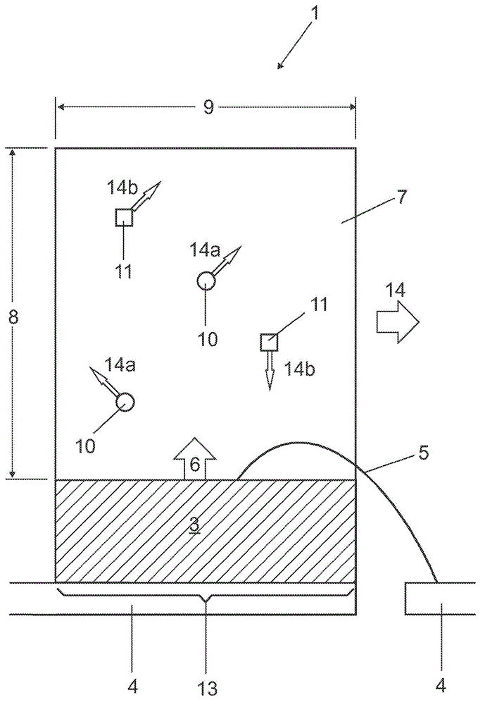
[0055] figure 1 The optoelectronic device 1 is shown. The semiconductor chip 3 is applied on the carrier 2. The electrical contact is achieved via the contact 4 and the bonding wire 5. The semiconductor chip 3 emits primary radiation 6. The semiconductor chip 3 is at least partially surrounded by an at least partially transparent medium 7 having a height 8 above the carrier 2 and a width 9 (aspect ratio) along the carrier 2. The particles 10, 11 that interact with the primary radiation 6 are introduced into the medium 7. Medium 7 has an aspect ratio greater than one. The particles 10, 11 are uniformly distribut...
PUM
 Abstract
Description
Claims
Application Information
 - R&D
- Intellectual Property
- Life Sciences
- Materials
- Tech Scout
- Unparalleled Data Quality
- Higher Quality Content
- 60% Fewer Hallucinations
Browse by: Latest US Patents, China's latest patents, Technical Efficacy Thesaurus, Application Domain, Technology Topic, Popular Technical Reports.
© 2025 PatSnap. All rights reserved.Legal|Privacy policy|Modern Slavery Act Transparency Statement|Sitemap|About US| Contact US: help@patsnap.com