Groove type field oxide power MOS (metal oxide semiconductor) device with ultra low conduction resistance

A MOS device, on-resistance technology, applied in semiconductor devices, electrical components, circuits, etc., can solve the problems of reducing device on-resistance, low on-resistance, reducing carrier drift distance, etc., to reduce drift distance, The effect of reducing the on-resistance

Active Publication Date: 2015-03-25
宝应县顺扬刺绣厂
View PDF4 Cites 0 Cited by
  • Summary
  • Abstract
  • Description
  • Claims
  • Application Information

AI Technical Summary

Problems solved by technology

[0004] In view of this, in order to further reduce the on-resistance of power MOS and alleviate the problem between device breakdown voltage and on-resistance, the present invention proposes a slot-type field oxygen power MOS device with extremely low on-resistance, which is more conventional The slot oxygen structure greatly reduces the drift distance of carriers, thereby effectively reducing the on-resistance of the device in the on state

Method used


Image

  • Groove type field oxide power MOS (metal oxide semiconductor) device with ultra low conduction resistance
  • Groove type field oxide power MOS (metal oxide semiconductor) device with ultra low conduction resistance
  • Groove type field oxide power MOS (metal oxide semiconductor) device with ultra low conduction resistance

Examples


Embodiment Construction

[0023] The preferred embodiments of the present invention will be described in detail below in conjunction with the accompanying drawings; it should be understood that the preferred embodiments are only for illustrating the present invention, rather than limiting the protection scope of the present invention.

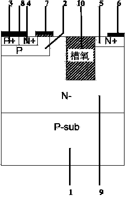
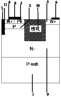
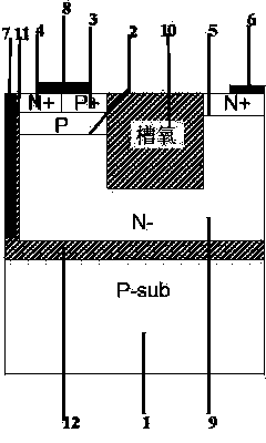
[0024] Figure 4 The present invention proposes a slot-type field oxygen power MOS device structure with extremely low on-resistance. As shown in the figure: a very low on-resistance trench field oxygen power MOS device structure provided by the present invention includes a substrate P-type silicon layer, an active top silicon layer and a trench field oxygen, and the active silicon layer contains Vertical channel 11, N-drift region 9, P-type silicon region 12, and N+ drain region 13 buried in the surface of the entire substrate P-type silicon layer 1, the vertical channel is arranged above the N-type silicon region, the The N-drift region is in contact with the P-type ...


PUM


Abstract

The invention discloses a groove type field oxide power MOS (metal oxide semiconductor) device with ultra low conduction resistance, relating to a semiconductor power device. The groove type field oxide power MOS device comprises a P-type silicon layer on a substrate, an active top silicon layer and groove type field oxide, wherein the active top silicon layer comprises a vertical channel, an N- drifting zone, a P-type silicon zone and a N+ drain zone buried in the surface of the whole substrate. Since the N+ drain zone is buried in the surface of the whole substrate based on the conventional groove type field oxide device, a current carrier can move directly through the N- drifting zone between the drain zone N+ and a source zone N+ when the device is in an ON state. Compared with the conventional groove type field oxide structure, the drifting distance of the current carrier can be reduced greatly, so that the conduction resistance of the device in the ON state can be reduced effectively. The structure is also suitable for power devices based on the SOI (silicon-on-insulator) technology.

Description

technical field [0001] The invention relates to a semiconductor power device, in particular to a slot-type field oxygen power MOS device with extremely low conduction resistance. Background technique [0002] Power MOS (Metal-Oxide-Semiconductor) devices are widely used in the field of power integration, and the contradiction between breakdown voltage and on-resistance has been one of the focal issues that people have been paying attention to for a long time. There are many solutions to alleviate this contradiction, among which the slot-type field oxygen structure is considered to be one of the structures that can effectively alleviate this contradiction. A typical conventional trough field oxygen structure such as figure 1 As shown, 1 is the substrate silicon layer, 2 is the P well, 3 is the P+ source region, 4 is the N+ source region, 5 is the N+ drain region, 6 is the drain electrode, 7 is the gate electrode, 8 is the source electrode, and 9 is the N-drift region, 10 is...

Claims


Application Information

Patent Timeline
Patent Type & Authority Patents(China)
IPC IPC(8): H01L29/06H01L29/78
Inventor 胡盛东张玲甘平周喜川周建林刘海涛
Owner 宝应县顺扬刺绣厂
Why Eureka
Try Eureka