
Reverse side engineered III-nitride devices

A technology of nitride and nitride layer, which is applied in the manufacture of semiconductor devices, electrical solid state devices, semiconductor/solid state devices, etc., and can solve problems such as difficulty in achieving high-quality buffer layers

Active Publication Date: 2012-10-03
TRANSPHORM INC
View PDF10 Cites 28 Cited by
  • Summary
  • Abstract
  • Description
  • Claims
  • Application Information

AI Technical Summary

Problems solved by technology

While this method produces acceptable spacers, channel and barrier layers, it is difficult to achieve high quality buffer layers

Method used


Image

  • Reverse side engineered III-nitride devices
  • Reverse side engineered III-nitride devices
  • Reverse side engineered III-nitride devices

Examples


Embodiment Construction

[0020] Techniques are described herein that enable the formation of Ill-nitride-type devices using silicon-based substrates.

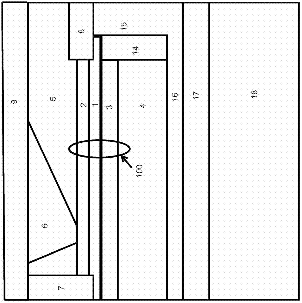
[0021] As used herein, the front or device side is the wafer or epitaxial layer on which a lateral device is fabricated by forming electrodes that make ohmic and / or Schottky and / or metal-insulator-semiconductor (MIS) contacts with the semiconductor face. The reverse side is opposite to the front or device side. As used herein, the term "III-nitride material" or "III-N material" means according to the stoichiometric formula Al x In y Ga zA compound semiconductor material of N where x+y+z is equal to 1 or approximately 1. The devices described here are Group III planar devices. However, the techniques described here can be applied to N-face devices with appropriate changes to the relative positions of the 2DEG layers and the type of the layer (ie, whether the layer is p-type or n-type or intrinsic). As used herein, "active layer(s)" is a set of III...


PUM


Abstract

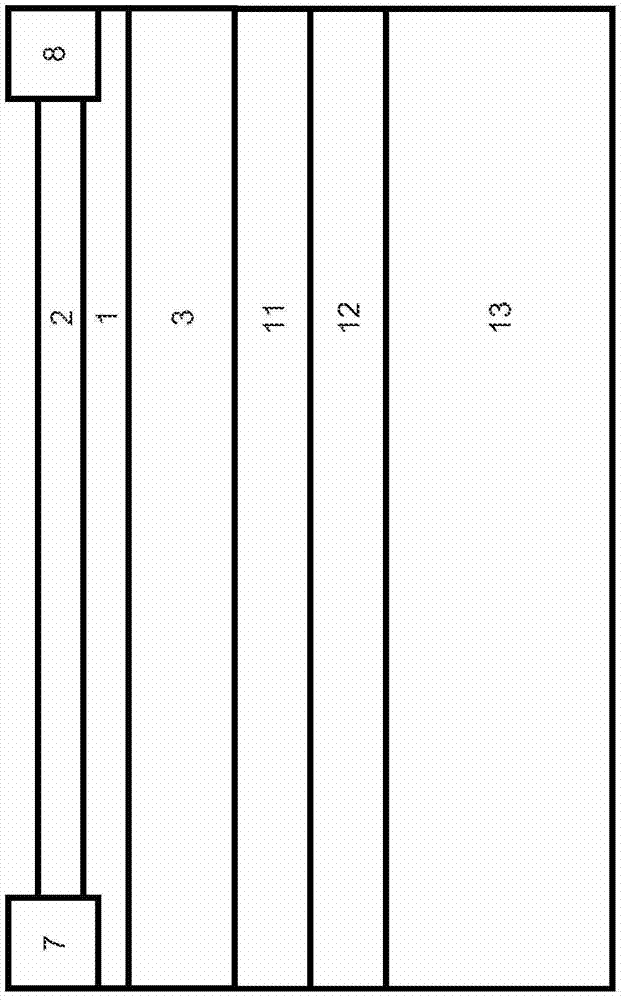
Group III-nitride devices are described that include a stack of III-nitride layers, passivation layers, and conductive contacts. The stack includes a channel layer with a 2DEG channel, a barrier layer and a spacer layer. One passivation layer directly contacts a surface of the spacer layer on a side opposite to the channel layer and is an electrical insulator. The stack of III-nitride layers and the first passivation layer form a structure with a reverse side proximate to the first passivation layer and an obverse side proximate to the barrier layer. Another passivation layer is on the obverse side of the structure. Defected nucleation and stress management layers that form a buffer layer during the formation process can be partially or entirely removed.

Description

technical field [0001] The present invention relates to a semiconductor device fabricated on a group III nitride semiconductor. Background technique [0002] For high-power electronic device applications, III-nitride-based devices have many potential material advantages over silicon-based devices. Among others, these include larger bandgap and breakdown fields, high electron mobility in two-dimensional electron gas (2DEG), low thermal generation current and the possibility to use direct bandgap, plus in many Various energy band and polarization design techniques can be applied in these structures for novel device functions. However, applications are hampered by the lack of low-cost substrates for device fabrication. [0003] Devices are sometimes formed by heteroepitaxy on suitable substrates such as silicon carbide, sapphire, or silicon. Techniques for applying the layers can include molecular beam epitaxy (MBE) or metal organic chemical vapor deposition (MOCVD) and hydr...

Claims


Application Information

Patent Timeline
Patent Type & Authority Applications(China)
IPC IPC(8): H01L29/778H01L21/335
CPCH01L24/06H01L29/7786H01L2224/03002H01L23/291H01L24/02H01L29/42316H01L2924/13064H01L29/66462H01L24/03H01L2224/03464H01L2224/04042H01L2224/03462H01L29/4175H01L2924/01029H01L2224/06183H01L2924/1032H01L29/2003H01L2224/94H01L21/0254H01L23/3171H01L2924/12032H01L2924/13062H01L2924/12042H01L2224/03H01L2924/00H01L29/6609H01L29/861
Inventor 储荣明乌梅什·米什拉拉柯许·K·拉尔
Owner TRANSPHORM INC
Learn More