Liquid crystal display device and manufacturing method thereof
A technology of a liquid crystal display device and a manufacturing method, which is applied in the fields of optics, instruments, nonlinear optics, etc., and can solve problems such as disturbance of voltage response characteristics and degradation
- Summary
- Abstract
- Description
- Claims
- Application Information
AI Technical Summary
Problems solved by technology
Method used
Image
Examples
Embodiment approach 1
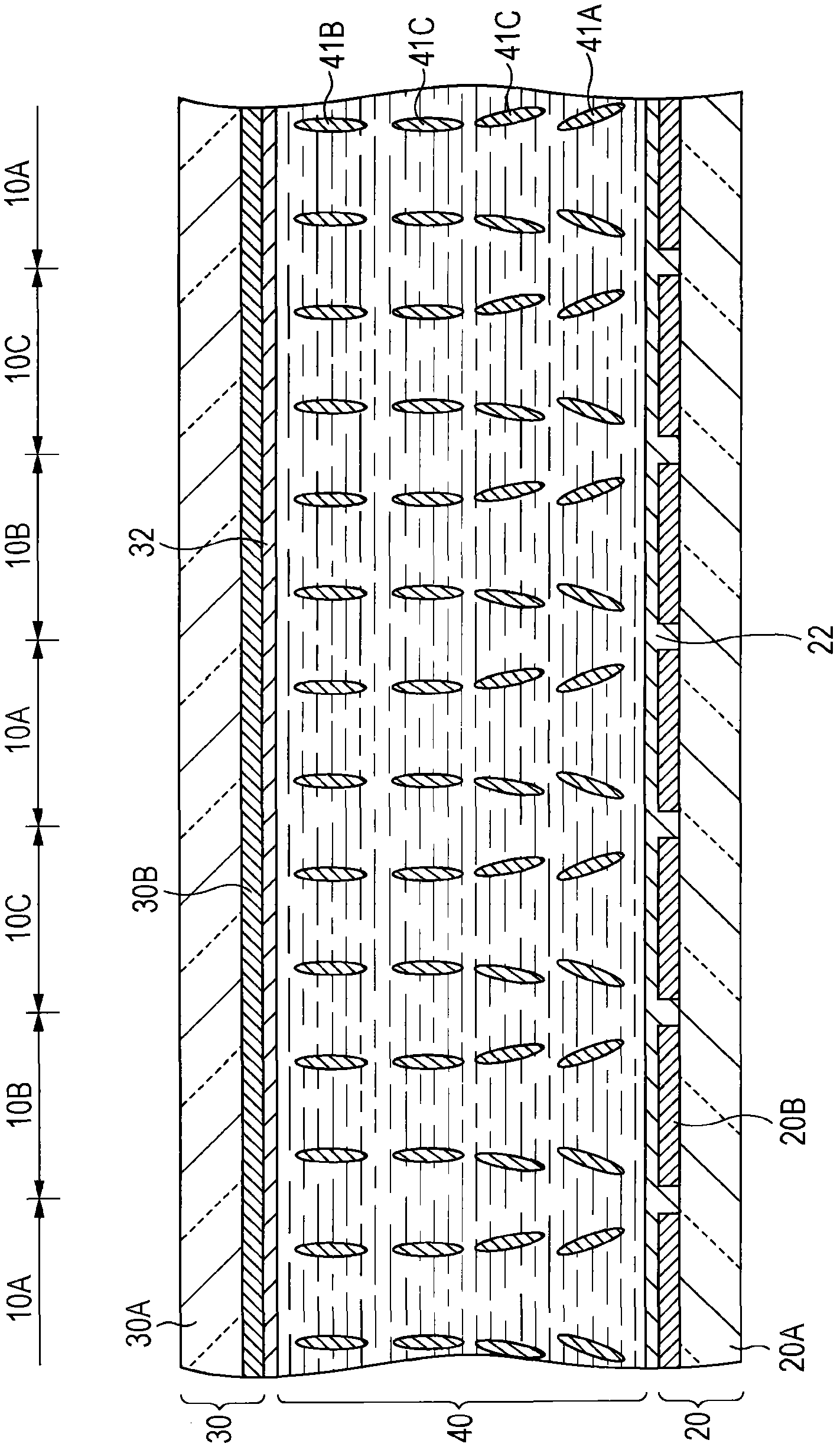
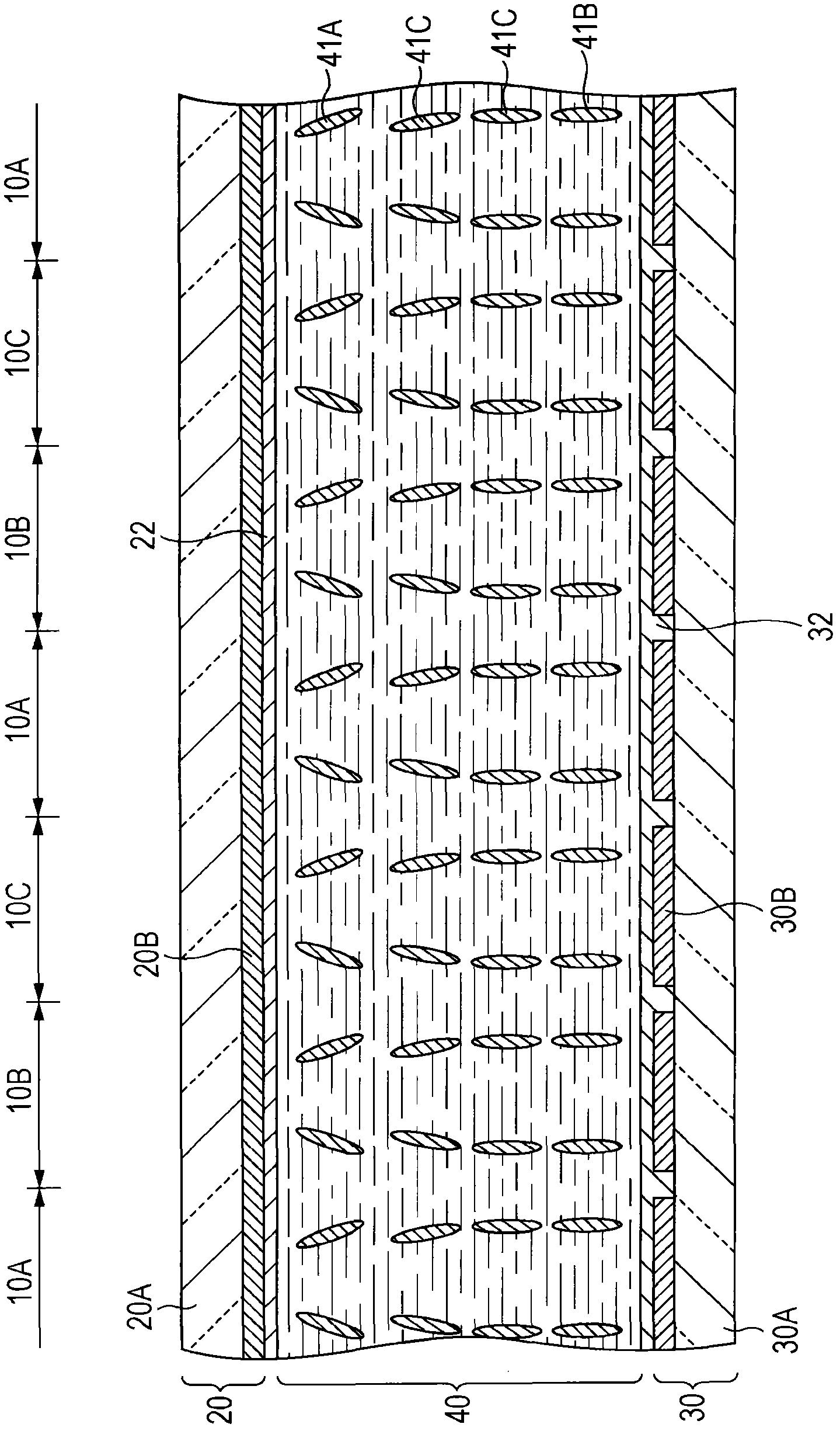
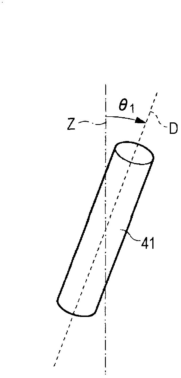
[0123] Embodiment 1 relates to a VA-mode liquid crystal display device (or liquid crystal display element) according to the first embodiment of the present invention and relates to a liquid crystal display device (or liquid crystal display element) according to the first embodiment or the third embodiment of the present invention. Manufacturing method. In Embodiment 1, the first alignment film 22 includes a compound obtained by crosslinking or polymerizing a polymer compound (compound before alignment treatment) having a crosslinkable functional group or a polymerizable functional group as a side chain (compound after alignment treatment); The second alignment film 32 includes the same compound as the compound constituting the first alignment film. That is, the first alignment film 22 and the second alignment film 32 are composed of the same polymer compound. In addition, the pretilt is imparted on the liquid crystal molecules by cross-linked or polymerized compounds. Here, ...
Embodiment approach 2
[0246] Embodiment 2 is a modified example of Embodiment 1. FIG. In the liquid crystal display device of Embodiment 2, the first alignment regulation portion 21 is provided on the first electrode (pixel electrode) 20B, and the first alignment film 22 covers the first electrode (pixel electrode) 20B, the first alignment regulation portion 21 and the opposite surface of the first substrate (TFT substrate) 20. A schematic partial cross-sectional view of a liquid crystal display device according to Embodiment 2 of the present invention is shown in Figure 8 middle.
[0247] More specifically, the first slit portion 21 (portion on which no electrode is formed) having a striped or V-shaped pattern is provided, for example, in each pixel of the pixel electrode 20B. Here, an arrangement diagram of the first electrode (pixel electrode) 20B and the first slit portion 21 when the pixel is viewed from above is shown in Figure 10A and 10B middle. Thus, when a driving voltage is applie...
Embodiment approach 3
[0262] Embodiment 3 relates to the liquid crystal display device according to the second embodiment of the present invention, and relates to the manufacturing method of the liquid crystal display device according to the second embodiment and the third embodiment of the present invention.
[0263] In Embodiment 1, the compound after alignment treatment is obtained by crosslinking or polymerizing the crosslinkable functional group or polymerizable functional group in the compound before alignment treatment containing a crosslinkable functional group or polymerizable functional group as a side chain. On the other hand, in Embodiment 3, the first alignment film 22 contains a compound obtained by deforming a polymer compound containing a photosensitive functional group as a side chain (a compound after alignment treatment), and the second alignment film 32 contains The same compound (compound after alignment treatment) as the compound (compound after alignment treatment) of the firs...
PUM
| Property | Measurement | Unit |
|---|---|---|
| Particle size | aaaaa | aaaaa |
Abstract
Description
Claims
Application Information
 - R&D
- Intellectual Property
- Life Sciences
- Materials
- Tech Scout
- Unparalleled Data Quality
- Higher Quality Content
- 60% Fewer Hallucinations
Browse by: Latest US Patents, China's latest patents, Technical Efficacy Thesaurus, Application Domain, Technology Topic, Popular Technical Reports.
© 2025 PatSnap. All rights reserved.Legal|Privacy policy|Modern Slavery Act Transparency Statement|Sitemap|About US| Contact US: help@patsnap.com


