Monitoring method of selective extension process

An epitaxy and selective technology, applied in electrical components, semiconductor/solid-state device manufacturing, circuits, etc., can solve the problem of high monitoring costs and achieve the effect of reducing monitoring costs

Active Publication Date: 2012-07-11
SEMICON MFG INT (SHANGHAI) CORP +1
View PDF4 Cites 1 Cited by
  • Summary
  • Abstract
  • Description
  • Claims
  • Application Information

AI Technical Summary

Problems solved by technology

This makes the monitoring of selective epitaxy process expensive

Method used


Image

  • Monitoring method of selective extension process
  • Monitoring method of selective extension process
  • Monitoring method of selective extension process

Examples


Embodiment Construction

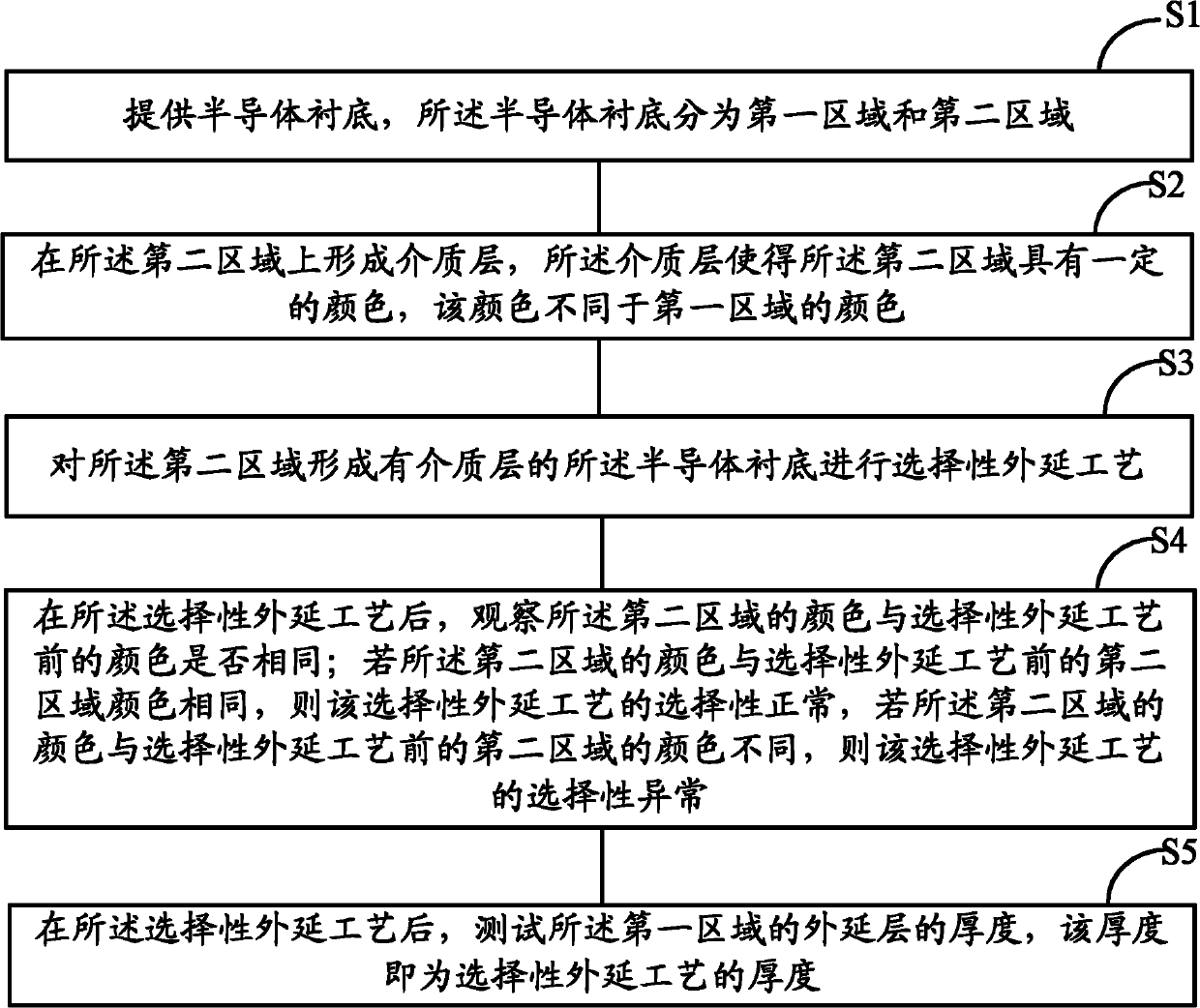
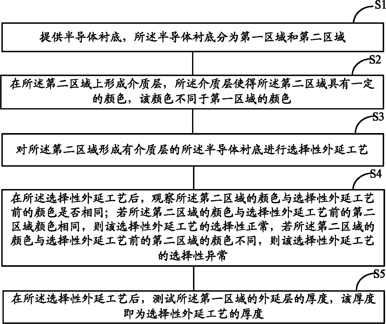
[0029] Since the prior art utilizes two semiconductor substrates to separately test the selectivity and thickness of the selective epitaxy process, the monitoring cost of the existing selective epitaxy process is relatively high. The invention uses two regions of the same semiconductor substrate to monitor separately, thereby realizing the monitoring of the selectivity and thickness of the selective epitaxy process with one semiconductor substrate, and reducing the monitoring cost of the selective epitaxy process.

[0030] Specifically, for the selective epitaxial process monitoring method of the present invention, please refer to figure 1 As shown, the method includes:

[0031] Step S1, providing a semiconductor substrate, the semiconductor substrate is divided into a first region and a second region;

[0032] Step S2, forming a dielectric layer on the second region, the dielectric layer makes the second region have a certain color, which is different from the color of the f...


PUM

PropertyMeasurementUnit
Thicknessaaaaaaaaaa

Abstract

The invention provides a monitoring method of selective extension process, which comprises steps of providing a semiconductor substrate provided with a first area and a second area; forming a medium layer enabling the second area to have color different from the first area on the second area; conducting the selective extension process on the semiconductor substrate; observing whether the color of the second area is same with that before conducting the selective extension process after the selective extension process is conducted; determining selectivity of the selective extension process to be accurate if the color of the second area is same with that of the second area before conducting the selective extension process, conversely determining the selectivity of the selective extension process to be abnormal; and testing epitaxial layer thickness of the first area after the selective extension process. The testing epitaxial layer thickness is the thickness of the selective extension process. The monitoring method tests the selectivity and the thickness of the selective extension process by using the same semiconductor substrate, and reduces cost of the selective extension monitoring process.

Description

technical field [0001] The invention relates to the technical field of semiconductors, in particular to a monitoring method for a selective epitaxy process. Background technique [0002] The epitaxial (Epitaxy, Epi) process refers to growing an epitaxial layer having the same lattice arrangement as the semiconductor substrate on the semiconductor substrate. According to different growth methods, the epitaxy process can be divided into two types: selective epitaxy (Selective Epi) and non-selective epitaxy (Blanket Epi, also known as full epitaxy). Among them, the non-selective epitaxial process will not only form an epitaxial layer on the surface of the semiconductor substrate, but also form an epitaxial layer on the surface of the silicon nitride layer and the metal layer on the semiconductor substrate; the selective epitaxial process will only form an epitaxial layer on the surface of the semiconductor substrate. The epitaxial layer is formed, and the epitaxial layer will ...

Claims


Application Information

Patent Timeline
IPC IPC(8): H01L21/20H01L21/66H01L21/00
Inventor 三重野文健涂火金何永根何有丰
Owner SEMICON MFG INT (SHANGHAI) CORP
Why Eureka
Try Eureka