Optical anti-counterfeiting element

An optical anti-counterfeiting and component technology, applied in the direction of diffraction gratings, identification devices, instruments, etc., can solve the problems of not easy holography, integrated application of interference light-variable features, unfavorable identification, weakening interference light-variable features, etc., to achieve good anti-counterfeiting, Effects with a wide variety of colors

Active Publication Date: 2015-04-29
ZHONGCHAO SPECIAL SECURITY TECH +1
View PDF6 Cites 1 Cited by
  • Summary
  • Abstract
  • Description
  • Claims
  • Application Information

AI Technical Summary

Problems solved by technology

The period of the holographic grating is on the order of microns, which is larger than the wavelength of visible light. Therefore, the combination of holography and interference optical change has an optical effect of the simple superposition of the two effects, and no new effect is produced, and the two effects interact with each other. , which weakens the interfering light-variable feature, which is not conducive to identification, so it is only suitable for small-area use of optical-variable anti-counterfeiting components as one of the features, and is not suitable for large-area use
[0004] The application with the publication number CN101699323A discloses another optical anti-counterfeiting element with a grating layer structure. The grating layer is a single-layer dielectric film with a two-dimensional surface relief grating. The anti-counterfeiting element has an obvious optical change effect when observed under a polarizer. However, because it adopts a single-layer dielectric film structure, the light-changing effect is single, only red and green changes, and it is not easy to integrate with holographic and interference light-changing features.

Method used


Image

  • Optical anti-counterfeiting element
  • Optical anti-counterfeiting element
  • Optical anti-counterfeiting element

Examples


Embodiment Construction

[0016] The optical anti-counterfeiting element according to the present invention will be described in detail below with reference to the accompanying drawings.

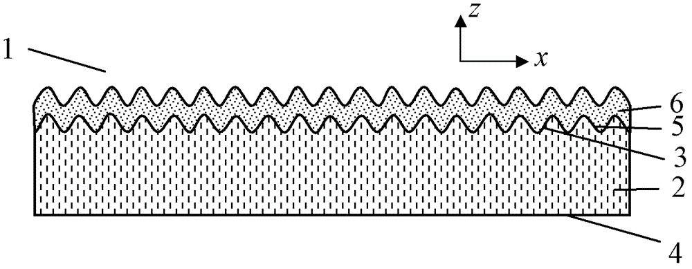
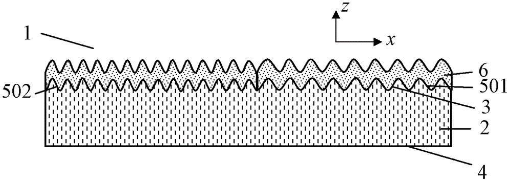
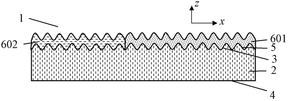
[0017] Such as figure 1 As shown, the optical anti-counterfeiting element 1 according to one embodiment of the present invention includes a substrate 2, the substrate 2 includes a first surface 3 and a second surface 4, and the optical anti-counterfeiting element also includes The sub-wavelength relief structure 5 on the first surface 3 and the multi-layer structure coating 6 formed on all or part of the sub-wavelength relief structure 5, and the multi-layer structure coating 6 is formed by a dielectric material with a refractive index less than 1.8 medium layer.

[0018] By matching the parameters of the sub-wavelength relief structure 5 and the multi-layer structure coating 6, the optical anti-counterfeiting element 1 according to the present invention can have a sub-wavelength relief structure 5 in the area of ​​...


PUM


Abstract

The invention provides an optical anti-counterfeiting element capable of overcoming the defect of few color types of the current optical anti-counterfeiting element. The optical anti-counterfeiting element comprises a substrate (2), a sub-wavelength embossment structure (5) and a coating (6) with a multi-layer structure, wherein the substrate (2) comprises a first surface (3) and a second surface (4); the sub-wavelength embossment (5) is formed on all or a part of the first surface (3); and the coating (6)with the multi-layer structure is formed on all or a part of the sub-wavelength embossment structure (5) and comprise a dielectric layer formed by dielectric material with refractive index less than 1.8.

Description

technical field [0001] The invention relates to the field of optical anti-counterfeiting, in particular to an optical anti-counterfeiting element. Background technique [0002] Today, optically variable technology is widely used in the public anti-counterfeiting of high-security securities such as banknotes. Device imitation or duplication. [0003] Chinese Patent Publication Nos. 1360544, 1423598 and 1617805 disclose optical anti-counterfeiting elements with various structures and optical interference characteristics and holography. Their common feature is that the metal reflective layer in the usual hologram is replaced by an optical interference film, or the interference optical variable image and hologram are located on both sides of the transparent layer or film, so that the interference optical variable feature and the holographic feature appear in the same area at the same time, Can produce some unique optical effects. The period of the holographic grating is on th...

Claims


Application Information

Patent Timeline
Patent Type & Authority Patents(China)
IPC IPC(8): G02B5/18G09F3/02B42D25/30B42D25/324
Inventor 孙凯王晓利张巍巍朱军
Owner ZHONGCHAO SPECIAL SECURITY TECH
Why Eureka
Try Eureka