Probe card structure

A probe card and probe unit technology, applied in the field of probe cards, can solve problems such as affecting the contact state of the elastic probe, poor flatness of the substrate, easy deformation or damage of the substrate, etc.

Inactive Publication Date: 2012-05-30
PLEADER YAMAICHI
View PDF4 Cites 7 Cited by
  • Summary
  • Abstract
  • Description
  • Claims
  • Application Information

AI Technical Summary

Problems solved by technology

However, the locking element clamped around the substrate is likely to cause slight bending of the substrate. If coupled with the reaction force of the elastic probe in the central area, the substrate is easily deformed or damaged. The larger the substrate, the more serious this problem. ; In addition, the poor flatness of the curved substrate will also affect the contact state of the elastic probe, and the uneven pressure and reaction force will cause the difference in the degree of damage of the elastic probe; therefore, the inventor aims at the above problems. Based on years of experience, this probe card structure is designed

Method used


Image

  • Probe card structure
  • Probe card structure
  • Probe card structure

Examples


Embodiment Construction

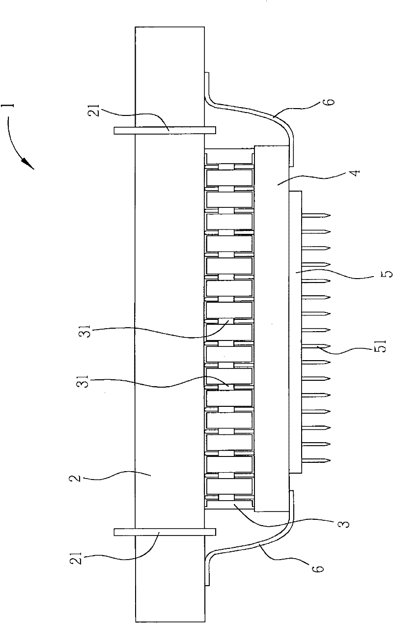
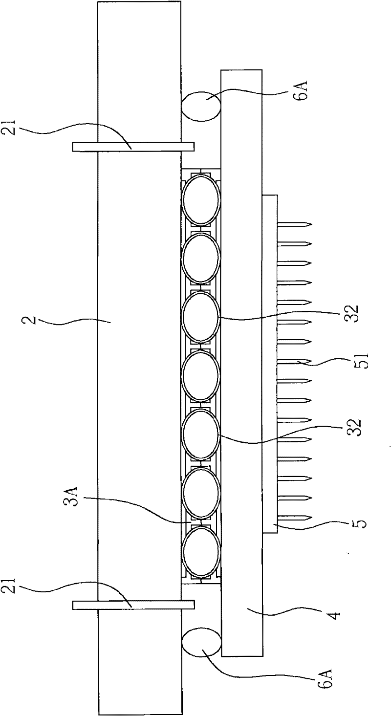
[0022] Such as figure 1 Shown is a cross-sectional view of the present invention. The probe card 1 of the present invention mainly includes a circuit board 2, an electrical connection device 3, a substrate 4, at least one probe unit 5, and a sealing rubber gasket 6.

[0023] The upper and lower surfaces of the circuit board 2 are formed with contact pads (not shown). The upper surface of the contact pad is electrically connected to the test head of a test device, and the lower surface of the contact pad is matched with the substrate 4 . The circuit board 2 is provided with at least one vacuum tube 21 penetrating the main body, and the position of the vacuum tube 21 is adjacent to or directly above the position of the substrate 4. The top of the vacuum tube 21 is connected to a vacuum pump via a pipeline, but it is not shown in the figure.

[0024] The electrical connection device 3 is arranged between the substrate 4 and the circuit board 2 as a signal transmission medium between...


PUM


Abstract

The invention discloses a probe card structure which mainly comprises a circuit board, an electrical connection apparatus, a substrate, at least a probe unit and a seal cushion. The probe unit is provided on the substrate with line distribution. The electrical connection apparatus is provided between the circuit board and the substrate, thus a signal can be transmitted between the circuit board and the probe unit. The seal cushion is provided between a lower surface of the circuit board and the substrate, periphery of the substrate and adjacent area of the circuit board are enclosed, thus pressure in space between the circuit board and the substrate is at a vacuum or negative pressure state, and the circuit board, the electrical connection apparatus and the substrate can stay in tight to be fixed together. Through design of the present invention, each member maintains a good electrical connection state, damage of members is reduced, when carrying out necessary maintenance, the members of the circuit board, the substrate and the like can be separated conveniently, and a service life of a product is prolonged.

Description

Technical field [0001] The present invention belongs to the technical field of a probe card, and particularly refers to a probe card used in a probe card with a large number of probes and a small spacing, and the components of the probe card are tightly fixed together by the principle of vacuum suction. Background technique [0002] With the maturity and improvement of technology, chip functions have gradually increased, designs have become increasingly complex, and the number of chip input / output pins has continued to increase. In order to reduce production costs, the size of wafers is constantly increasing (such as 12 o'clock wafers), so the demand for probe cards for large-area detection is gradually increasing. For such large-area probe cards, due to the small distance between the probe contact points, a multilayer substrate with circuits is usually used in the structure to be arranged between multiple probes and the circuit board as a space conversion device for the circuit....

Claims


Application Information

Patent Timeline
IPC IPC(8): G01R1/067G01R1/073G01R1/04
Inventor 古仁丁黄郑隆刘育宗
Owner PLEADER YAMAICHI
Why Eureka
Try Eureka