Method for driving plasma display panel and plasma display device
A technology of display panel and driving method, which is applied to static indicators, instruments, etc., and can solve problems such as sustain electrode-data electrode redundant discharge, etc.
- Summary
- Abstract
- Description
- Claims
- Application Information
AI Technical Summary
Problems solved by technology
Method used
Image

Examples
Embodiment approach 1
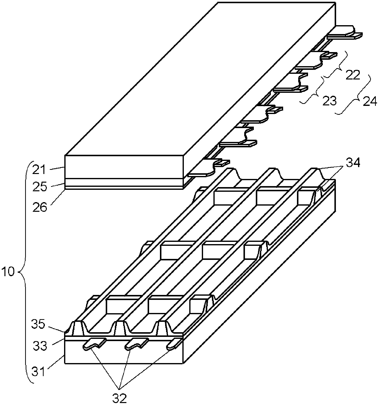
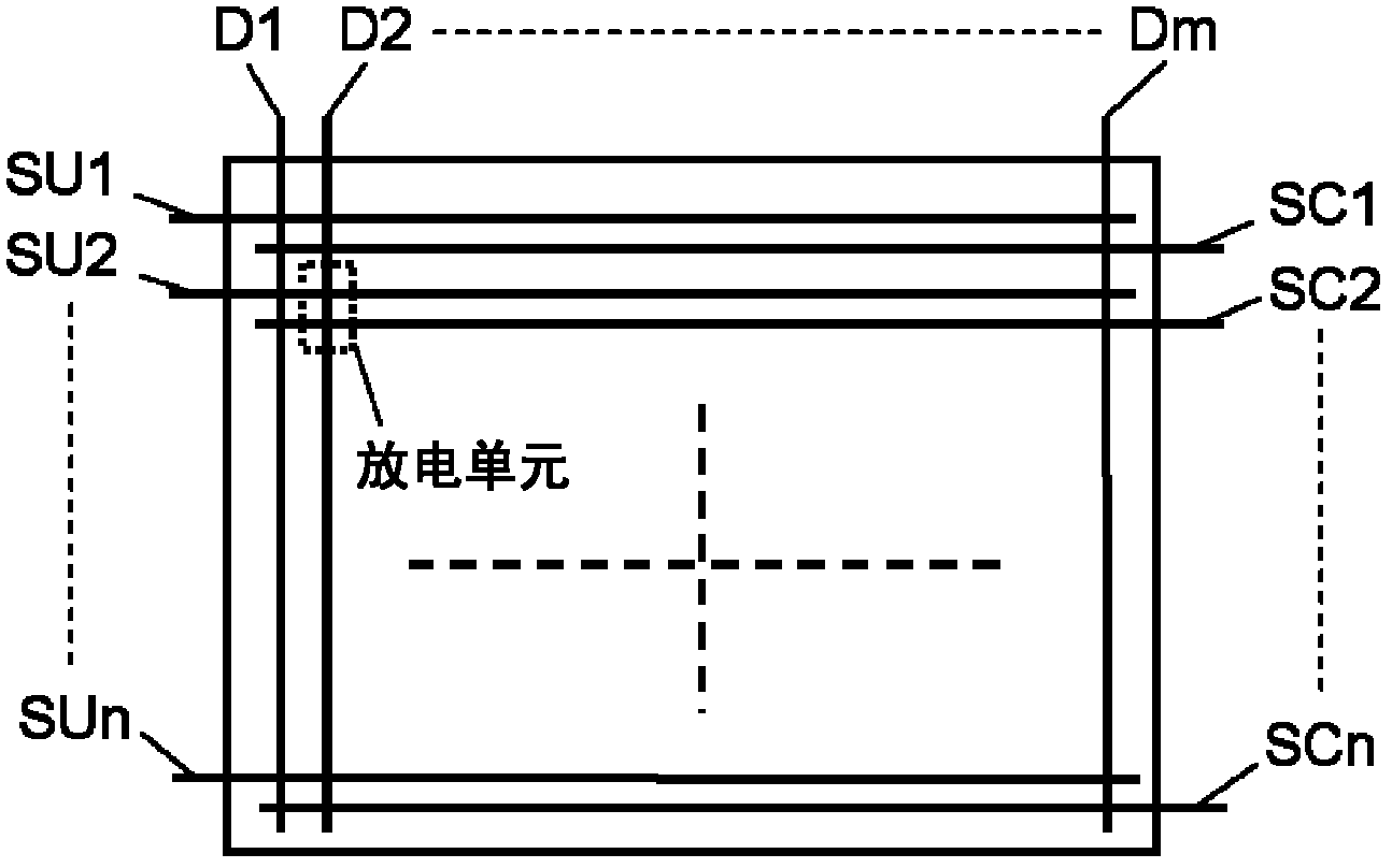
[0037] figure 1 It is an exploded perspective view showing the structure of the panel 10 in Embodiment 1 of this invention. A plurality of display electrode pairs 24 including scan electrodes 22 and sustain electrodes 23 are formed on glass front panel 21 . Furthermore, dielectric layer 25 is formed to cover scan electrodes 22 and sustain electrodes 23 , and protective layer 26 is formed on dielectric layer 25 . In addition, the protective layer 26 is formed of a material mainly composed of magnesium oxide (MgO), which has a high secondary electron emission coefficient and is excellent in durability.
[0038] A plurality of data electrodes 32 are formed on rear plate 31 , dielectric layer 33 is formed to cover data electrodes 32 , and wellhead-shaped partition walls 34 are formed on dielectric layer 33 . Further, phosphor layers 35 that emit light in each color of red (R), green (G) and blue (B) are provided on the side surfaces of the barrier ribs 34 and the dielectric laye...
Embodiment approach 2
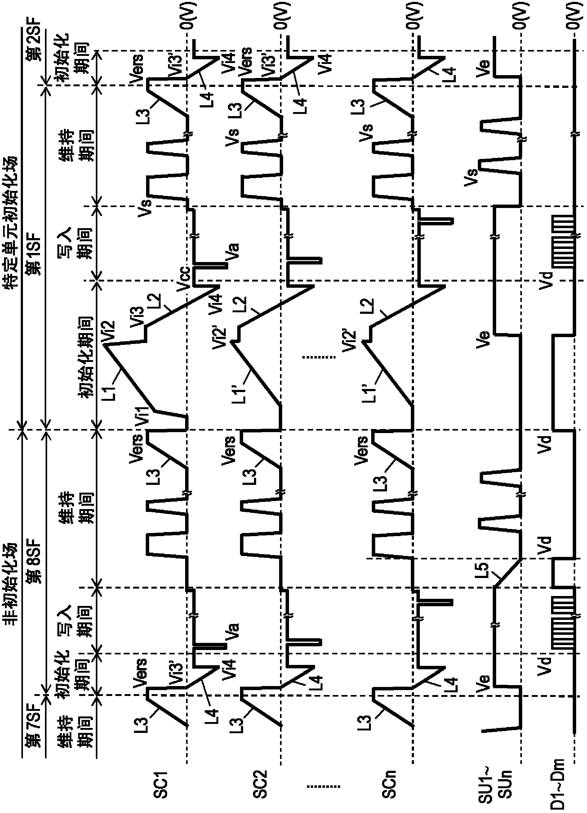
[0182] In Embodiment 1, the down-slope voltage L5 was shown as a waveform shape that falls with a constant gradient, but the down-slope voltage in the present invention is not limited to this waveform shape at all. For example, the downhill voltage may have a waveform shape having two slope regions with mutually different slopes.
[0183] Figure 10 It is a waveform diagram showing an example of a driving voltage waveform applied to each electrode of panel 10 in Embodiment 2 of the present invention. Figure 10 The drive voltage waveform shown with the image 3 The drive voltage waveform shown is different in that, instead of the downhill voltage L5, a downhill voltage L5' having a waveform shape having two slope regions with mutually different slopes is used.
[0184] In the present embodiment, down-ramp voltage L5' applied to sustain electrode 23 is generated in a waveform shape that drops sharply until discharge occurs in the discharge cell, and then falls gradually after...
Embodiment approach 3
[0195] In Embodiment 1, an example of a structure in which the forced initializing operation is performed only once in a plurality of fields in each discharge cell is described, and the method for stabilizing the addressing operation of the discharge cell that does not perform the forced initializing is described. Effect. However, the present invention is not limited to this structure at all, and can also be applied to other subfield structures.
[0196] Figure 12 It is a waveform diagram showing an example of a driving voltage waveform applied to each electrode of panel 10 in Embodiment 3 of the present invention. exist Figure 12 In the driving voltage waveform shown, the first SF is assumed to be an all-cell initializing subfield in which a forced initializing operation is performed in all discharge cells. For example, even in this case, it is possible to prevent unnecessary discharge from being generated in the discharge cell when the positive voltage Vd is applied to ...
PUM
 Abstract
Description
Claims
Application Information
 - R&D
- Intellectual Property
- Life Sciences
- Materials
- Tech Scout
- Unparalleled Data Quality
- Higher Quality Content
- 60% Fewer Hallucinations
Browse by: Latest US Patents, China's latest patents, Technical Efficacy Thesaurus, Application Domain, Technology Topic, Popular Technical Reports.
© 2025 PatSnap. All rights reserved.Legal|Privacy policy|Modern Slavery Act Transparency Statement|Sitemap|About US| Contact US: help@patsnap.com