Microcrystalline low-temperature lens and camera using same
A low-temperature, microcrystalline technology, applied in the field of low-temperature lenses, can solve problems that cannot be completely eliminated, and achieve the effects of simple and practical system design, avoiding changes, and simple working principles
- Summary
- Abstract
- Description
- Claims
- Application Information
AI Technical Summary
Problems solved by technology
Method used
Image
Examples
Embodiment
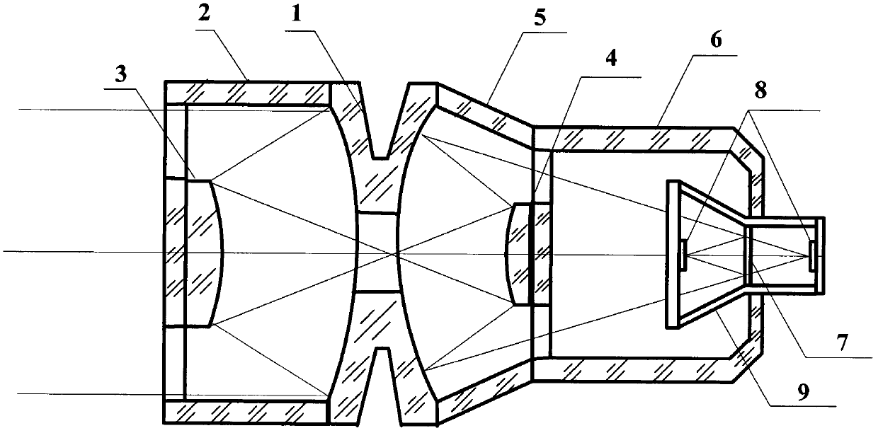
[0034] The working spectrum of the all-microcrystalline lens is B1: 5.0~7.6μm, B2: 8.2~12.0μm, entrance pupil diameter: 300mm, F number 1.5, effective field of view is 4°; detector B1 spectrum and B2 spectrum pixels The size is 30μm area array CCD. The primary mirror / four mirrors (1) are concave hyperboloid mirrors, the secondary mirror (3) is convex hyperboloid mirrors, and the third mirror (4) is a convex spherical mirror.
[0035] The working environment temperature for processing, assembly and testing is 293K, and the working environment temperature is 120K.
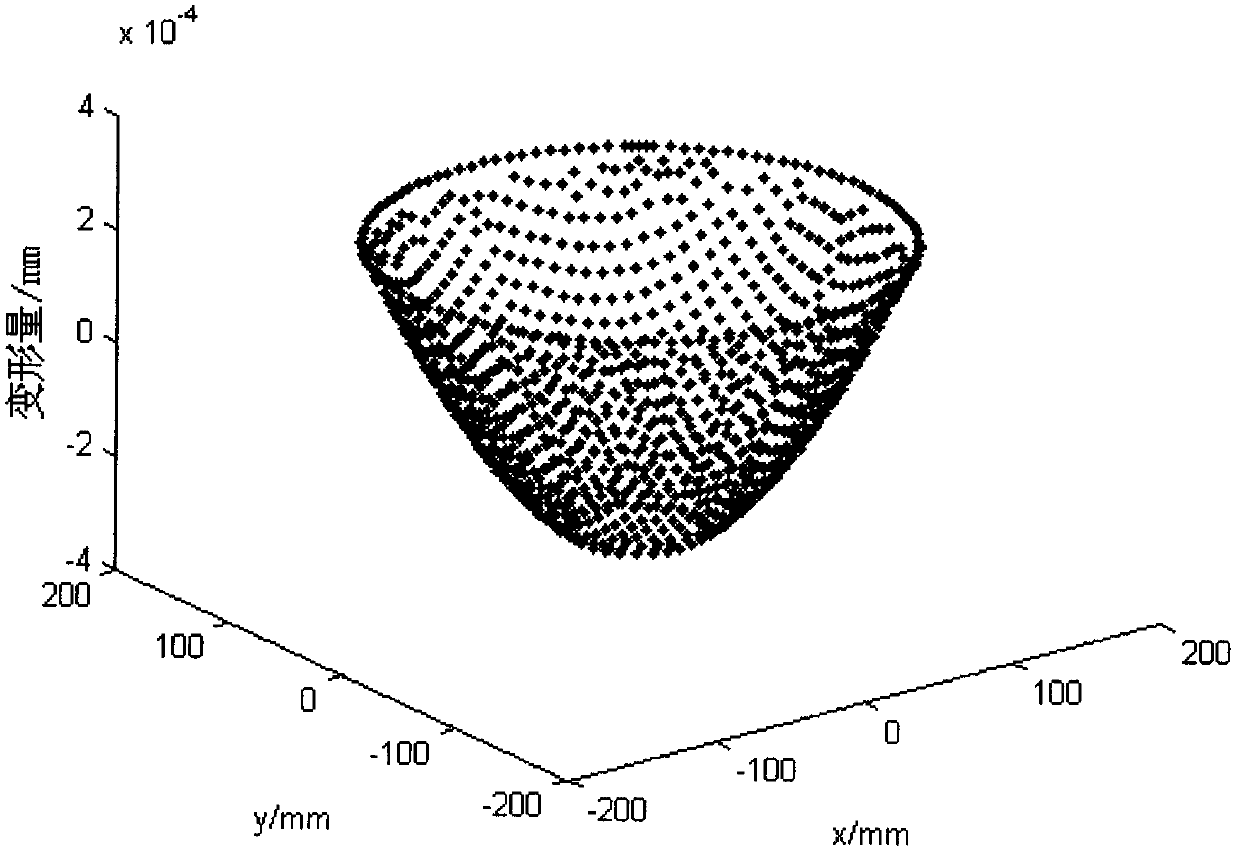
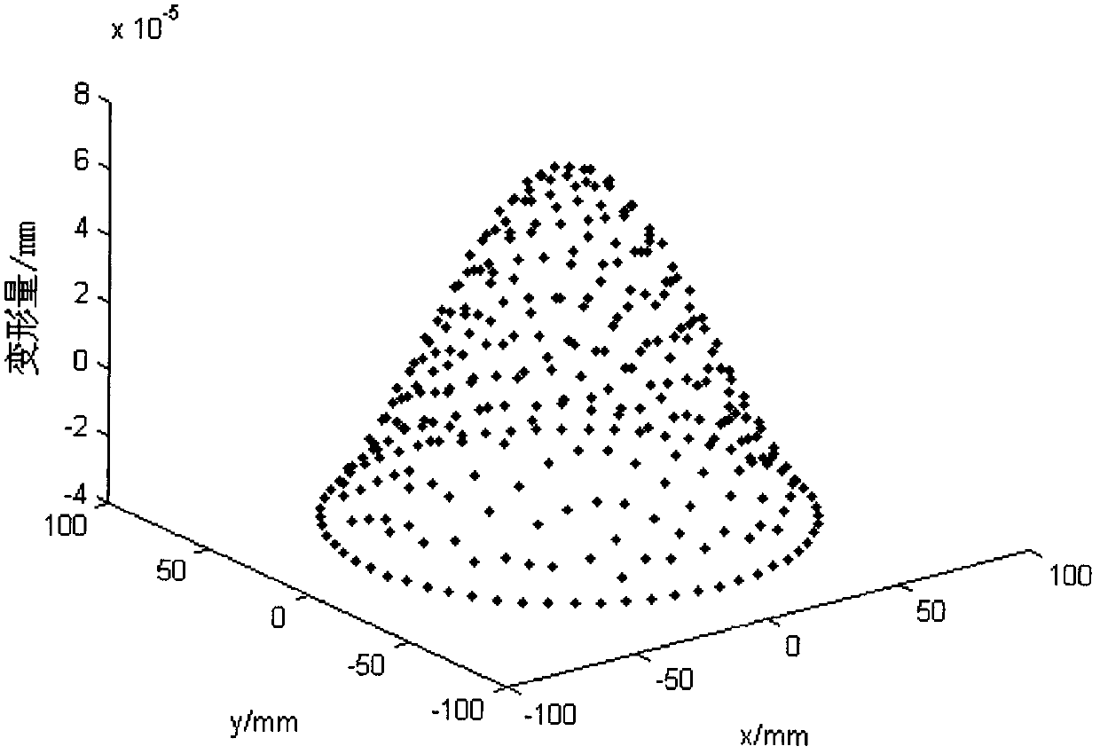
[0036] In this embodiment, when the temperature drops from 293K to 120K, the deformation of each mirror surface of the all-microcrystalline cryogenic lens is as Figure 2a~2d As shown, the deformation of each mirror surface is symmetrical.
[0037] In this embodiment, the pixel energy concentration of the B1 and B2 spectrum bands of the all-microcrystalline cryogenic lens under 293K and 120K working conditions is as follow...
PUM
 Abstract
Description
Claims
Application Information
 - R&D Engineer
- R&D Manager
- IP Professional
- Industry Leading Data Capabilities
- Powerful AI technology
- Patent DNA Extraction
Browse by: Latest US Patents, China's latest patents, Technical Efficacy Thesaurus, Application Domain, Technology Topic, Popular Technical Reports.
© 2024 PatSnap. All rights reserved.Legal|Privacy policy|Modern Slavery Act Transparency Statement|Sitemap|About US| Contact US: help@patsnap.com


