PLL circuit for reducing reference leak and phase noise
A phase comparison circuit and circuit technology, applied in the direction of electrical components, automatic power control, etc., can solve problems such as dead zones, and achieve the effects of preventing phase errors, shortening locking time, and preventing output error phase errors
- Summary
- Abstract
- Description
- Claims
- Application Information
AI Technical Summary
Problems solved by technology
Method used
Image
Examples
Embodiment approach 1
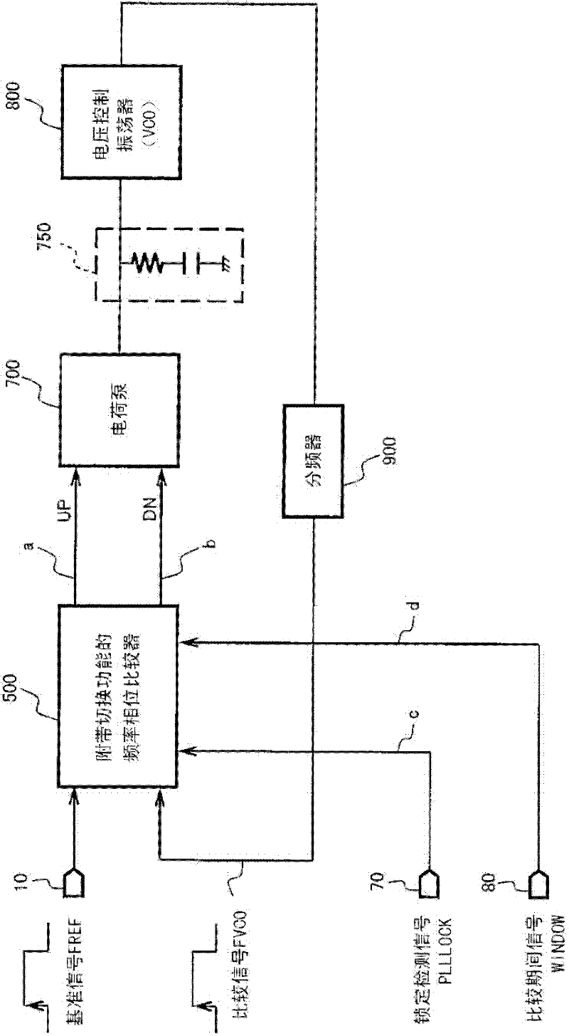
[0084] exist figure 1 The structure of the PLL circuit in Embodiment 1 of the present invention is shown in . This PLL circuit includes a frequency-phase comparator 500 with a switching function, a charge pump 700 , a loop filter 750 , a voltage controlled oscillator (VCO) 800 , and a frequency divider 900 for dividing the output of the voltage controlled oscillator 800 .
[0085] The VCO 800 controls its oscillation frequency according to the voltage of the loop filter 750 , and the loop filter 750 charges and discharges the capacitors constituting the loop filter 750 through the output current of the charge pump 700 , and its voltage changes accordingly. The phase error output signal (UP signal and DN signal) output from the frequency-phase comparator 500 with switching function is input to the charge pump 700 , and a current corresponding to the phase error output signal is output. The frequency-phase comparator 500 with switching function inputs the reference signal FREF...
Embodiment approach 2
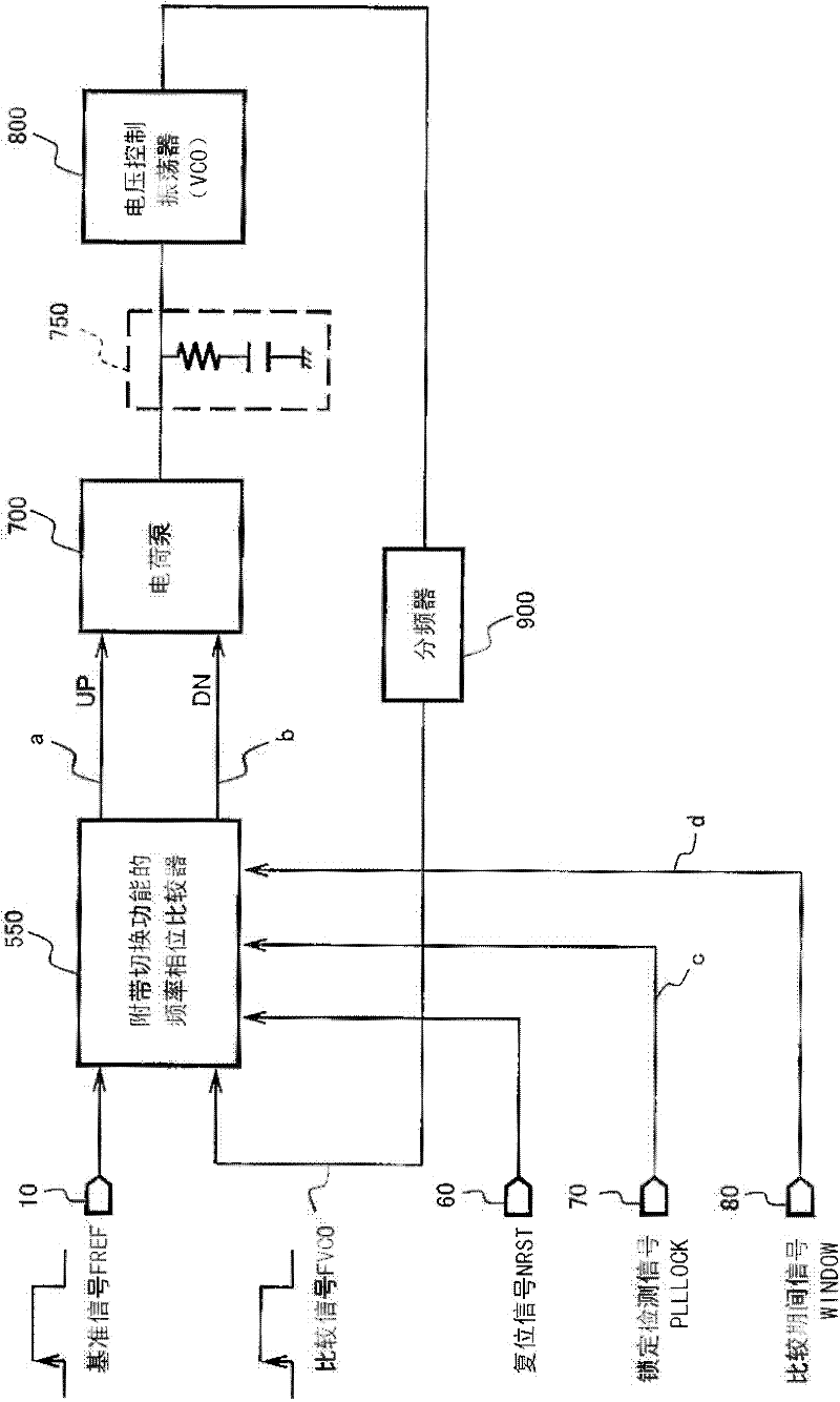
[0127] exist figure 2 A configuration diagram of a PLL circuit in Embodiment 2 of the present invention is shown in . In this embodiment, the same reference numerals are assigned to the same configurations as those in Embodiment 1, and description thereof will be omitted. In the PLL circuit of the present embodiment, instead of the frequency-phase comparator circuit 500 with a switching function in the PLL circuit of the first embodiment, a frequency-phase comparator 550 with a switching function provided with a reset input terminal is arranged.
[0128] exist Figure 5 Expressed in figure 2 The internal structure of the frequency-phase comparator 550 with switching function in the shown PLL circuit. Such as Figure 5 As shown, the frequency-phase comparator 550 of this embodiment is configured to input the reset signal NRST60 to the frequency comparison circuit 350 . exist Figure 11 Expressed in Figure 5 The internal structure of the frequency comparison circuit is...
Embodiment approach 3
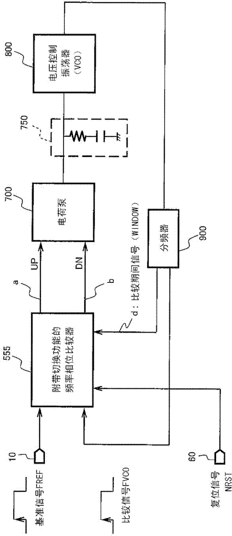
[0137] exist image 3 A block diagram of a PLL circuit in Embodiment 3 of the present invention is shown in . In the present embodiment, the same reference numerals are assigned to the same configurations as those in the second embodiment, and description thereof will be omitted.
[0138] The PLL circuit in this embodiment differs from Embodiment 2 in that it includes a lock detection signal generator 600, and a frequency phase comparator 555 with a switching function generates a lock detection signal PLLLOCK in accordance with the comparison period signal WINDOW80 and the reference signal FREF10. .
[0139] exist Figure 6 said in image 3 The internal structure diagram of the frequency-phase comparison 555 with switching function in the PLL circuit shown. Such as Figure 6 As shown, the comparison period signal WINDOW is input as a data signal and the reference signal FREF10 is input as a clock signal to the lock detection signal generation unit 600 .
PUM
 Abstract
Description
Claims
Application Information
 - Generate Ideas
- Intellectual Property
- Life Sciences
- Materials
- Tech Scout
- Unparalleled Data Quality
- Higher Quality Content
- 60% Fewer Hallucinations
Browse by: Latest US Patents, China's latest patents, Technical Efficacy Thesaurus, Application Domain, Technology Topic, Popular Technical Reports.
© 2025 PatSnap. All rights reserved.Legal|Privacy policy|Modern Slavery Act Transparency Statement|Sitemap|About US| Contact US: help@patsnap.com


