Mother substrate used for detecting winding of array and detecting method thereof
A mother substrate and array technology, which is applied in the field of the mother substrate of the test line group, can solve the problems of increased manufacturing cost, cost waste, and scrapped driver chips.
- Summary
- Abstract
- Description
- Claims
- Application Information
AI Technical Summary
Problems solved by technology
Method used
Image
Examples
no. 1 example
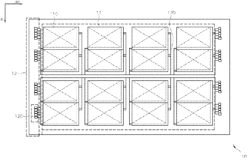
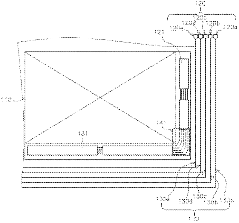
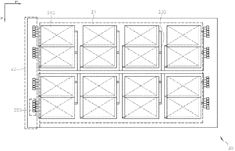
[0032] First please refer to figure 2 , and refer to Figure 2a , figure 2 is a schematic top view of the mother substrate of the present invention, Figure 2a It is a schematic diagram of the first embodiment of the connection structure between the lead wire and the test wire of the present invention, and it can also be regarded as an enlarged view of a single liquid crystal panel on the mother substrate. exist figure 2 Among them, a liquid crystal panel array 21 and a test area 22 are arranged on the mother substrate 20 . The liquid crystal panel array 21 is provided with a plurality of liquid crystal panels 210 , and the liquid crystal panels 210 are arranged in m rows and n columns in the liquid crystal panel array 21 , so the number is m×n. The test area 22 is provided with a plurality of test pad groups 220, and each test pad group 220 further includes a test pad 220a, a test pad 220b, a test pad 220c, a test pad 220d and a test pad 220e. A plurality of test line...
no. 2 example
[0037] again please refer to figure 2 , the difference in this embodiment lies in the connection structure of the lead wire and the test wire, please refer to Figure 2b .
[0038] Figure 2b It is a schematic diagram of the second embodiment of the connecting structure of the lead wire and the test wire of the present invention. exist Figure 2b Among them, there is a test line group 230 outside the liquid crystal panel 210, and the test line group 230 includes a test line 230a, a test line 230b, a test line 230c, a test line 230d and a test line 230e. At the same time, in order to make the motherboard 20 externally connected to the voltage through the test pad set 220, the test line set 230 is electrically connected to the test line set 220, specifically: the test line 230a is electrically connected to the test pad 220a, and the test line 230b is electrically connected to the test line set 220. The test line 230c is electrically connected to the test pad 220c, the test ...
no. 3 example
[0041] again please refer to figure 2 , the difference in this embodiment lies in the connection structure of the lead wire and the test wire, please refer to Figure 2c .
[0042] Figure 2c It is a schematic diagram of the third embodiment of the connecting structure of the lead wire and the test wire of the present invention. exist Figure 2c Among them, there is a test line group 230 outside the liquid crystal panel 210, and the test line group 230 includes a test line 230a, a test line 230b, a test line 230c, a test line 230d and a test line 230e. At the same time, in order to make the entire motherboard 20 externally connected to the voltage through the test pad set 214, the test line 230a is electrically connected to the test pad 220a, the test line 230b is electrically connected to the test pad 220b, and the test line 230c is electrically connected to the test pad 220c. , the test line 230d is electrically connected to the test pad 220d, and the test line 230e is ...
PUM
 Abstract
Description
Claims
Application Information
 - R&D
- Intellectual Property
- Life Sciences
- Materials
- Tech Scout
- Unparalleled Data Quality
- Higher Quality Content
- 60% Fewer Hallucinations
Browse by: Latest US Patents, China's latest patents, Technical Efficacy Thesaurus, Application Domain, Technology Topic, Popular Technical Reports.
© 2025 PatSnap. All rights reserved.Legal|Privacy policy|Modern Slavery Act Transparency Statement|Sitemap|About US| Contact US: help@patsnap.com


