
Chip circuit fan-out method and thin film chip device

A thin-film chip and chip technology, applied in circuits, electrical components, electrical solid devices, etc., can solve the problems of reducing the cost of chip design, etc., and achieve the effect of convenient line layout, overcoming line kinks, and large layout flexibility

Inactive Publication Date: 2015-11-25
NOVATEK MICROELECTRONICS CORP
View PDF6 Cites 0 Cited by
  • Summary
  • Abstract
  • Description
  • Claims
  • Application Information

AI Technical Summary

Problems solved by technology

[0005] However, either increasing the chip area or adjusting the position of bumps on the chip involves the re-layout of the integrated circuits inside the chip, which is not in line with the trend of shrinking the chip and reducing the design cost.

Method used


Image

  • Chip circuit fan-out method and thin film chip device
  • Chip circuit fan-out method and thin film chip device
  • Chip circuit fan-out method and thin film chip device

Examples


Embodiment Construction

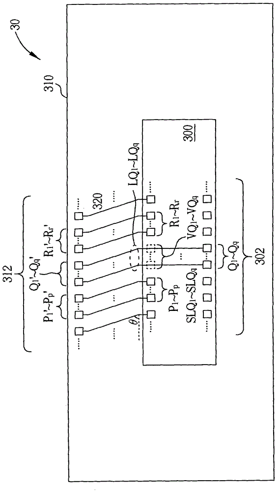
[0040] Different from the prior art that the joints of the external pins must be connected to the external protrusions in accordance with the arrangement order of the external protrusions, in the following embodiments, the joints of the external pins will not be connected in accordance with the arrangement order of the external protrusions To even the outer bumps. In other words, the corresponding relationship between the connection points of the outer pins and the outer protrusions is not equal to the corresponding relationship between the spatial arrangement. If clearly defined, the joints of the external pins are arranged according to a "corresponding sequence of protrusions", which represents the corresponding relationship between the joints of the external pins and the joints of the external protrusions in connection with each other, and the joints of the external protrusions The blocks are arranged according to a "arranging order of the outer protrusions", and the corres...


PUM


Abstract

A chip fanning out method is disclosed. The chip fanning out method includes mounting a chip on a film, forming a plurality of outer lead bonds spatially arranged in a bump correspondence order on the film, forming a plurality of bumps spatially arranged in a bump arrangement order on the chip, and forming a plurality of wires to connect the plurality of outer lead bonds to the plurality of bumps according to the bump correspondence order, wherein the bump correspondence order is different from the bump arrangement order.

Description

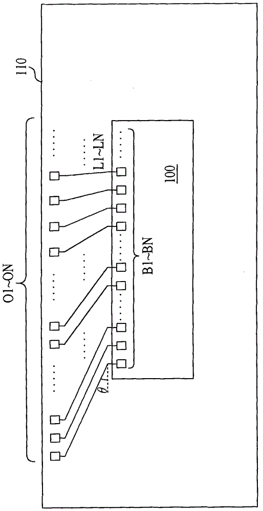
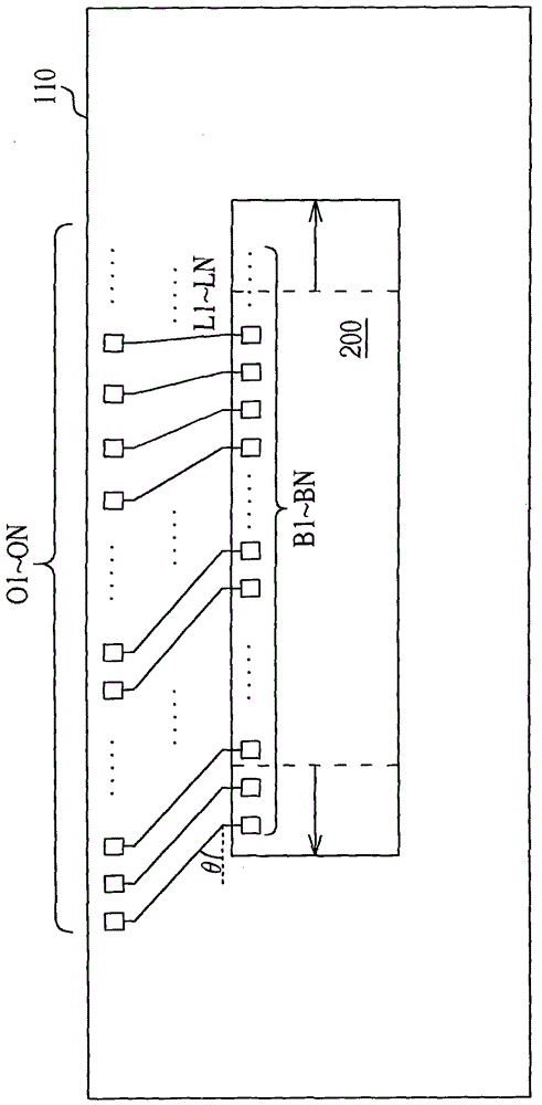
technical field [0001] The invention relates to a chip circuit fan-out method and a related thin film chip device. Background technique [0002] With the evolution of circuit manufacturing technology, integrated circuit chips are not limited to be mounted on traditional printed circuit boards (Printed Circuit Board, PCB), for example, integrated circuit chips can also be mounted on films. This packaging technology is called "chip on thin film" (ChiponFilm, COF) packaging technology. [0003] Please refer to figure 1 , figure 1 It is a schematic diagram of a fanout layout of a thin film chip package in the prior art. exist figure 1 Among them, the outer bumps B1-BN on a chip 100 are connected to the outer lead bonding points (Outer Lead Bond, OLB) O1-ON through the lines L1-LN on a thin film 110, and the outer lead bonding points O1 ~ON can be connected to hardware devices such as traditional printed circuit boards or liquid crystal display (LiquidCrystalDisplay, LCD) pa...

Claims


Application Information

Patent Timeline
Patent Type & Authority Patents(China)
IPC IPC(8): H01L21/60H01L21/50H01L23/498
CPCH01L2924/0002
Inventor 萧兆志李柏青
Owner NOVATEK MICROELECTRONICS CORP
Learn More