Liquid crystal display device
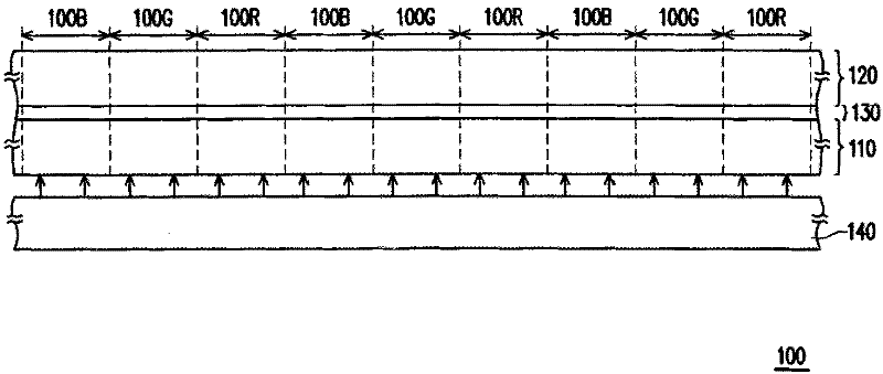
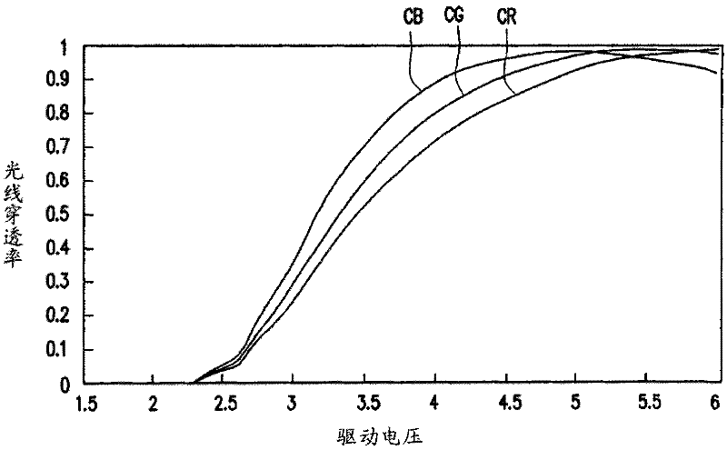
A technology of a liquid crystal display device and a liquid crystal layer, applied in nonlinear optics, instruments, optics, etc., capable of solving problems affecting the display quality of a liquid crystal display device 100, and achieving the effect of solving the problem of color distortion
- Summary
- Abstract
- Description
- Claims
- Application Information
AI Technical Summary
Problems solved by technology
Method used
Image
Examples
no. 1 example
[0091] Figure 3A A schematic partial cross-sectional view of a liquid crystal display device according to a first embodiment of the present invention is shown. Figure 3B based on Figure 3A A partial top view of the first substrate in . Please also refer to Figure 3A and Figure 3B , the liquid crystal display device 300 of this embodiment has a plurality of first pixel regions 300B, a plurality of second pixel regions 300G and a plurality of third pixel regions 300R, wherein Figure 3A and Figure 3B Only one first pixel region 300B, one second pixel region 300G and one third pixel region 300R are shown as an example. In addition, the liquid crystal display device 300 includes a first substrate 310 , a second substrate 320 and a liquid crystal layer 330 disposed between the first substrate 310 and the second substrate 320 .
[0092] The first insulating film 310M is disposed on the first substrate 310 in the first pixel region 300B, the second pixel region 300G and the...
no. 2 example
[0105] Figure 4 A schematic partial cross-sectional view of a liquid crystal display device according to a second embodiment of the present invention is shown. Please refer to Figure 4 , the liquid crystal display device 400 of this embodiment has a plurality of first pixel regions 400B, a plurality of second pixel regions 400G and a plurality of third pixel regions 400R, wherein Figure 4 Only one first pixel region 400B, one second pixel region 400G and one third pixel region 400R are shown as an example. In addition, the liquid crystal display device 400 includes a first substrate 410 , a second substrate 420 and a liquid crystal layer 430 disposed between the first substrate 410 and the second substrate 420 .
[0106] The first insulating film 410M is disposed on the first substrate 410 in the first pixel region 400B, the second pixel region 400G and the third pixel region 400R respectively. 1 , the second insulating film 410M 2 with the third insulating film 410M 3...
no. 3 example
[0116] Figure 5 A partial cross-sectional schematic diagram of a liquid crystal display device according to a third embodiment of the present invention is shown. Please refer to Figure 5 , the liquid crystal display device 500 of this embodiment has a plurality of first pixel regions 500B, a plurality of second pixel regions 500G and a plurality of third pixel regions 500R, wherein Figure 5 Only one first pixel region 500B, one second pixel region 500G and one third pixel region 500R are shown as an example. In addition, the liquid crystal display device 500 includes a first substrate 510 , a second substrate 520 and a liquid crystal layer 530 disposed between the first substrate 510 and the second substrate 520 .
[0117] The first insulating film 510M is disposed on the first substrate 510 in the first pixel region 500B, the second pixel region 500G and the third pixel region 500R respectively. 1 , the second insulating film 510M 2 with the third insulating film 510M ...
PUM
 Abstract
Description
Claims
Application Information
 - R&D Engineer
- R&D Manager
- IP Professional
- Industry Leading Data Capabilities
- Powerful AI technology
- Patent DNA Extraction
Browse by: Latest US Patents, China's latest patents, Technical Efficacy Thesaurus, Application Domain, Technology Topic, Popular Technical Reports.
© 2024 PatSnap. All rights reserved.Legal|Privacy policy|Modern Slavery Act Transparency Statement|Sitemap|About US| Contact US: help@patsnap.com


