


Quick Research
Generate reliable direction feasibility study reports for your R&D in just a few steps.

Technical Q&A
Discover and master advanced knowledge NOW. Basics, ideas, possibilities, all at once.

Find Solutions
As an expert in R&D theories, this can generate solutions to your technical problems instantly.

Evaluate Feasibility
Analyze your overall solution with one click, know your potential R&D risks in advance.

Monitor Landscape
Get weekly tech updates, stay abreast of the latest tech innovations and key insights.
Display apparatus
A technology for a display device and a display part, which is applied to identification devices, static indicators, optics, etc., can solve the problems of inability to prevent large-scale, complex device structure, etc., and achieves the effect of simple structure and prevention of display quality degradation.
- Summary
- Abstract
- Description
- Claims
- Application Information
AI Technical Summary
Problems solved by technology
Method used
Image

Examples
no. 1 approach
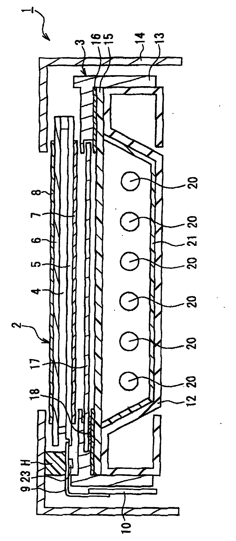
[0047] figure 1 It is a schematic cross-sectional view illustrating the liquid crystal display device according to the first embodiment of the present invention. exist figure 1 Among them, in the liquid crystal display device 1 of this embodiment, there are provided: the upper side of the figure as the viewing side (display surface side) and the liquid crystal panel 2 as the display part; and the non-display surface side of the liquid crystal panel 2. (lower side of the drawing), an illuminating device 3 that emits illuminating light for illuminating the liquid crystal panel 2 .
[0048] The liquid crystal panel 2 includes: a liquid crystal layer 4; an active matrix substrate 5 and a color filter substrate 6 as a pair of transparent substrates sandwiching the liquid crystal layer 4; Polarizers 7, 8 on the outer surfaces of each. In addition, a flexible printed circuit board 9 and a printed circuit board 10 connected to the flexible printed circuit board 9 are provided on th...
no. 2 approach
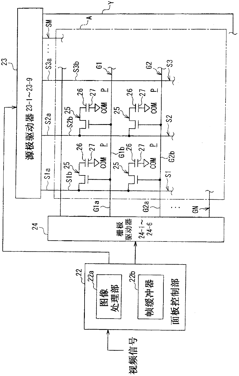
[0097] Figure 6 It is a diagram illustrating a configuration of a main part of a source driver in a liquid crystal display device according to a second embodiment of the present invention. In the figure, the main difference between this embodiment and the above-mentioned first embodiment is that a selector is provided between the sampling memory and the redundancy amplifier, and the selector connects only the source wiring connected to the redundancy wiring. The output corresponding data signal is selectively output to the redundant amplifier side. In addition, the same code|symbol is attached|subjected to the element common to the said 1st Embodiment, and the overlapping description is abbreviate|omitted.
[0098] That is, if Figure 6 As shown, in the present embodiment, the source driver (data wiring drive unit) 23 is provided with a sampling memory 41 as a storage unit; and a first latch 42 and an amplifier output unit 43 sequentially connected to the sampling memory 41...
PUM
| Property | Measurement | Unit |
|---|---|---|
| Thickness | aaaaa | aaaaa |
| Thickness | aaaaa | aaaaa |
Abstract
Description
Claims
Application Information
 - R&D Engineer
- R&D Manager
- IP Professional
- Industry Leading Data Capabilities
- Powerful AI technology
- Patent DNA Extraction
Browse by: Latest US Patents, China's latest patents, Technical Efficacy Thesaurus, Application Domain, Technology Topic, Popular Technical Reports.
© 2024 PatSnap. All rights reserved.Legal|Privacy policy|Modern Slavery Act Transparency Statement|Sitemap|About US| Contact US: help@patsnap.com