
Method for acquiring reference product yield of new product on production line

A new product and production line technology, applied in electrical components, semiconductor/solid-state device manufacturing, circuits, etc., can solve problems such as low product yield, high defect density, and inability to accurately predict new product benchmark product yields, etc. The effect of product yield

Inactive Publication Date: 2011-06-29
SEMICON MFG INT (SHANGHAI) CORP +1
View PDF0 Cites 10 Cited by
  • Summary
  • Abstract
  • Description
  • Claims
  • Application Information

AI Technical Summary

Problems solved by technology

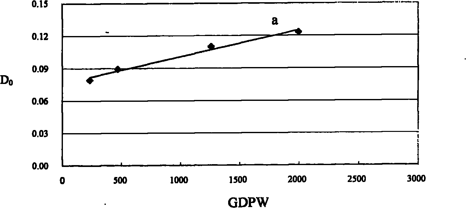
Although the formula (0.2) has already included the consideration of the chip size factor of different products, there are two problems in the practical application of this formula: (1) the chip with a small chip size has a large defect density, (2) the memory Chips with a large proportion of the area to the chip area have a high defect density
[0012] The reason why the defect density of products with a large proportion of the storage area to the chip area is that the circuit design of the storage area is usually the area with the densest device density on the chip, and some relatively small particles have little effect on other areas of the chip or even can Neglect; but for the storage area, due to the tight circuit layout, very small particles are likely to affect the product yield, which eventually leads to low product yield and high defect density for products with a large proportion of the storage area to the chip area
[0013] It can be seen from the above that the formula (0.2) cannot obtain the inherent defect density of the wafer production line, so it cannot accurately predict the yield rate of the benchmark product of the new product

Method used


Image

  • Method for acquiring reference product yield of new product on production line
  • Method for acquiring reference product yield of new product on production line
  • Method for acquiring reference product yield of new product on production line

Examples


Embodiment Construction

[0046] In order to make the object, technical solution, and advantages of the present invention clearer, the present invention will be further described in detail below with reference to the accompanying drawings and examples.

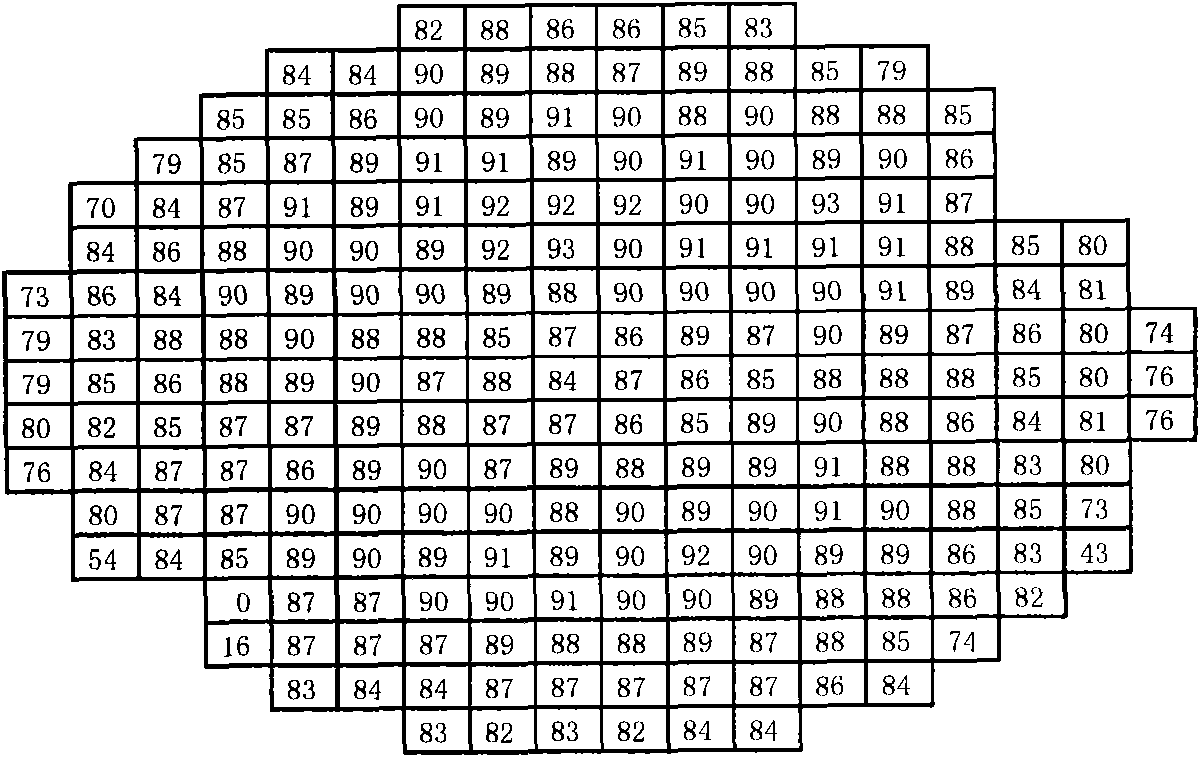
[0047] First, consider the impact of chip size on product yield, and use yield screening and misload rate compensation to remove the impact of chip size on product yield. Among them, yield screening solves the problem of wafer consistency, and misload rate compensation Solve non-defective failures. Secondly, the defect density correction factor is introduced based on the effect of the ratio of the storage area to the chip area on the defect density.

[0048] First, remove the impact of chip size on product yield, which is specifically divided into two aspects: wafer consistency screening and non-defect failure correction. specifically:

[0049] 1. Wafer consistency screening, get the corrected Yield’

[0050] The wafer consistency screening is divid...


PUM


Abstract

The invention provides a method for acquiring the reference product yield of a new product on a production line. The method comprises the following steps of: introducing yield screening, overkill rate compensation and a defect density correction coefficient; substituting in a defect density formula to obtain a defect density correction formula; and calculating to acquire the intrinsic defect density of the production line so as to accurately acquire the reference product yield of the new product on the production line.

Description

technical field [0001] The invention relates to the field of semiconductors, in particular to a method for obtaining the yield rate of a benchmark product of a new product in a production line. Background technique [0002] At present, the semiconductor manufacturing process is to grow hundreds of thousands of identical chips on a wafer at the same time, and the wafer after all the processes are completed is also called a bare chip. Qualified chips are selected by testing the bare chips, and cut and packaged into products. Usually, the method for calculating the product yield Yield of a certain product produced by a wafer production line is to first randomly select a number of dies of this product produced by the same wafer production line (the number can vary according to the production situation), and then test and select All the chips on all the dies, using Yield's calculation formula: [0003] Yield = number of qualified chips / total number of chips (0.1) [0004] Ge...

Claims


Application Information

Patent Timeline
Patent Type & Authority Applications(China)
IPC IPC(8): H01L21/00
Inventor 梅杰王立刘喆秋
Owner SEMICON MFG INT (SHANGHAI) CORP
Learn More