


Quick Research
Generate reliable direction feasibility study reports for your R&D in just a few steps.

Technical Q&A
Discover and master advanced knowledge NOW. Basics, ideas, possibilities, all at once.

Find Solutions
As an expert in R&D theories, this can generate solutions to your technical problems instantly.

Evaluate Feasibility
Analyze your overall solution with one click, know your potential R&D risks in advance.

Monitor Landscape
Get weekly tech updates, stay abreast of the latest tech innovations and key insights.
Characteristic inspection and classification apparatus for sheet-like electronic component
A technology for electronic components and sorting devices, which is applied in the direction of measuring devices, electrical components, circuits, etc., can solve the problems of rising pressure of the ejected gas, entering, and the inability to select and distinguish sheet electronic components, so as to prevent misclassification and high reliability Effect
- Summary
- Abstract
- Description
- Claims
- Application Information
AI Technical Summary
Problems solved by technology
Method used
Image

Examples
Embodiment 1
[0029] The size of the chip electronic component (type 0603) that is the object of the chip electronic component characteristic inspection and classification device is 0.6 mm long x 0.3 mm wide x 0.3 mm thick, and the minimum value of the outer dimension is 0.3 mm.
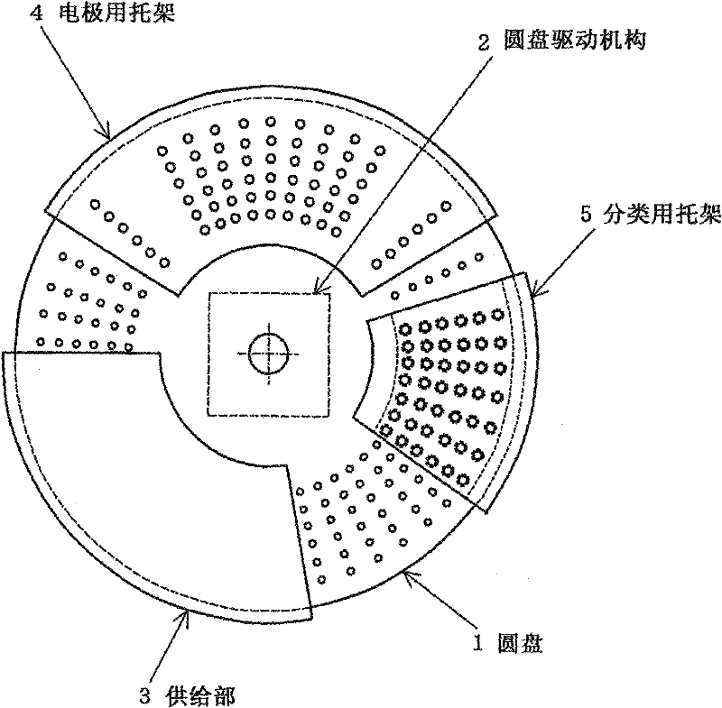
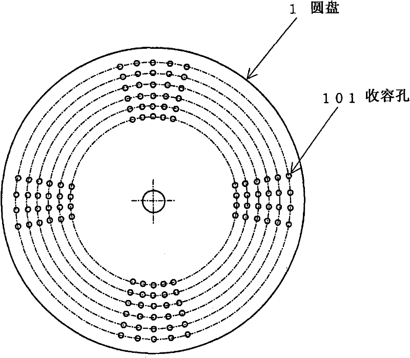
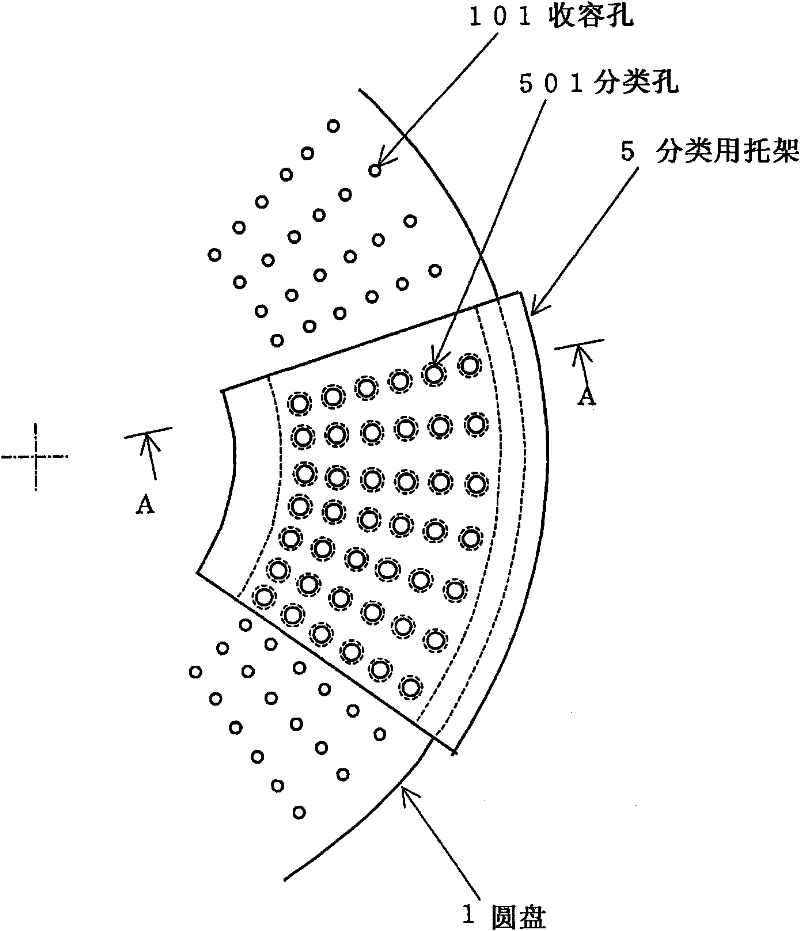
[0030] refer to image 3 , Figure 4 , Figure 5 and Image 6 A characteristic inspection and classification device for chip electronic components corresponding to Embodiment 1 of the present invention will be described. image 3 is to zoom in figure 1 A top view of a portion of the bracket used for sorting, Figure 4 It is viewed from the direction of arrow A in the diagram image 3 A cross-sectional view of the classification bracket, Figure 5 yes Figure 4 An enlarged view of the portion of the sorting hole shown, Image 6 It is an enlarged view of a conventional sorting hole portion, and is a figure for explaining occurrence of misclassification.
[0031] Such as image 3 , Figure 4 and Figure 5...
Embodiment 2
[0043] When the object of the chip electronic component characteristic inspection and classification device is set as a chip electronic component (1005 type), the minimum value of its external dimension is 0.5mm, so it is possible to set a predetermined value smaller than the minimum external dimension of the chip electronic component The length is set to 0.4 mm, for example.
Embodiment 3
[0045] When the object of the chip electronic component characteristic inspection and classification device is set as a chip electronic component (0402 type), the minimum value of its external dimension is 0.2mm, so it can be scheduled The length is set to 0.15 mm, for example.
[0046] Various modifications can be made within the scope of the present invention to the embodiments described in detail above. For example, a predetermined length smaller than the minimum value of the outer dimension of the chip electronic component may be selected according to the situation within the regulations. In addition, as clearly explained above, the effect of the present invention is also effective for chip-like electronic components having external dimensions other than the examples. At this time, what can be said for all the target chip electronic components is that the tip of the chip electronic component in the housing hole 101 of the target chip electronic component described in the ...
PUM
 Abstract
Description
Claims
Application Information
 - R&D Engineer
- R&D Manager
- IP Professional
- Industry Leading Data Capabilities
- Powerful AI technology
- Patent DNA Extraction
Browse by: Latest US Patents, China's latest patents, Technical Efficacy Thesaurus, Application Domain, Technology Topic, Popular Technical Reports.
© 2024 PatSnap. All rights reserved.Legal|Privacy policy|Modern Slavery Act Transparency Statement|Sitemap|About US| Contact US: help@patsnap.com