Solid-state imaging device and camera

A technology of solid-state imaging devices and imaging units, which is applied in the field of cameras, can solve problems such as image quality degradation, and achieve the effects of periodic degradation suppression and uniform pixel output signals

Inactive Publication Date: 2013-05-08
SONY SEMICON SOLUTIONS CORP
View PDF1 Cites 0 Cited by
  • Summary
  • Abstract
  • Description
  • Claims
  • Application Information

AI Technical Summary

Problems solved by technology

Therefore, since the photo-sensing units and the wiring layers are not regularly arranged, or in other words, since the pattern constituted by the photo-sensing units and the wiring layers is a non-uniform pattern, the sensitivity of each photo-sensing unit changes periodically, resulting in a loss from the solid-state imaging device. Periodic degradation of image quality in the output image signal

Method used


Image

  • Solid-state imaging device and camera
  • Solid-state imaging device and camera
  • Solid-state imaging device and camera

Examples


no. 1 example

[0040] 2. The second embodiment

[0041] 3. Modification

[0042] 1. The first embodiment

[0043] Schematic structure of a solid-state imaging device

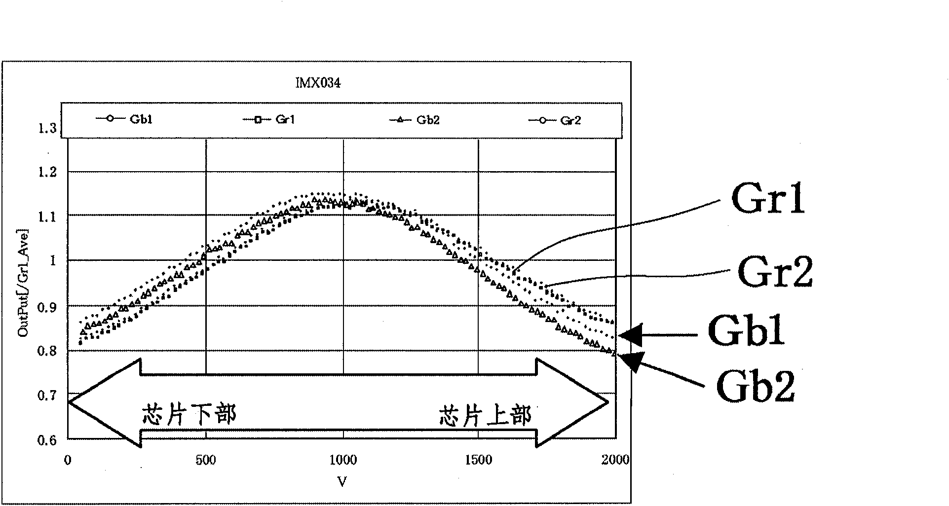
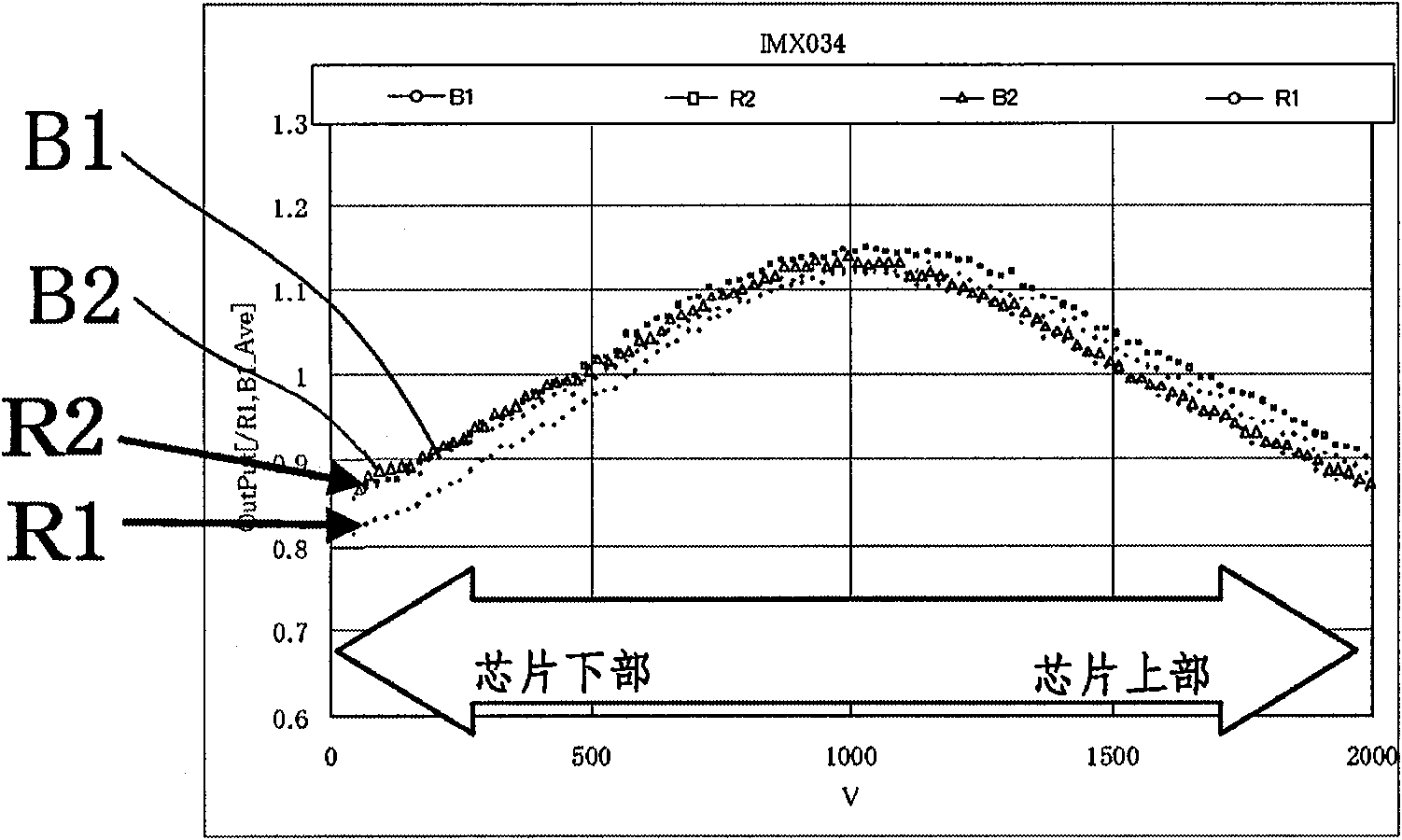
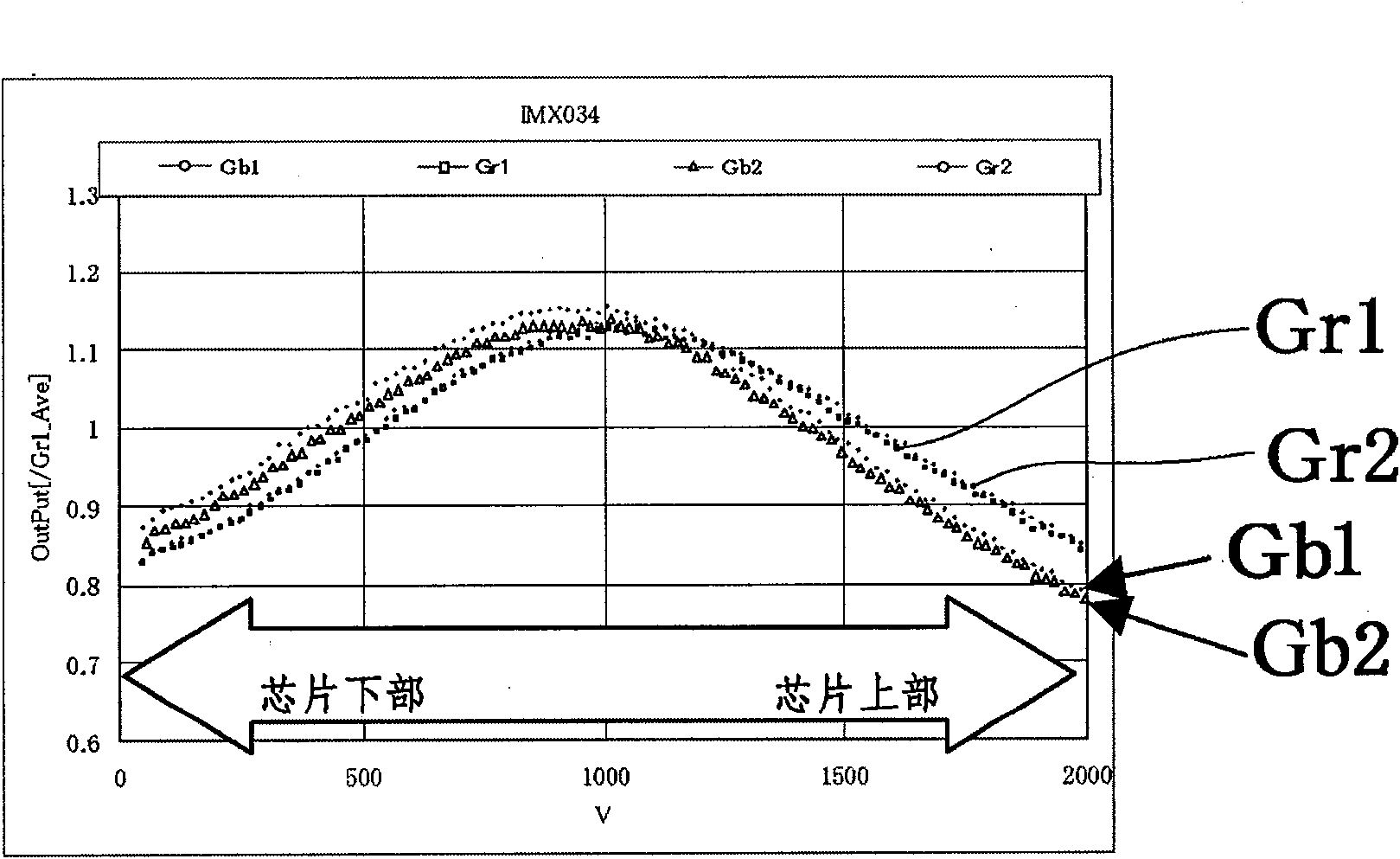
[0044] figure 1 is a schematic configuration diagram of a CMOS type image sensor as an example of a solid-state imaging device according to an embodiment of the present invention. exist figure 1 In the shown CMOS type image sensor, multiple sets of two pixels sharing the reset transistor Tr2, the amplification transistor Tr3, and the selection transistor Tr4 are arranged in a matrix form. Hereinafter, a group of two pixels that share the reset transistor Tr2 , the amplification transistor Tr3 , and the selection transistor Tr4 is referred to as a two-pixel common element unit.

[0045] More specifically, the two photodiodes PD1 and PD2 and the two transfer transistors Tr11 and Tr12 respectively corresponding to the photodiodes PD1 and PD2 share the reset transistor Tr2 , the amplification transistor Tr3 and the select...


PUM


Abstract

A solid-state imaging device includes: an imaging unit wherein a plurality of light sensing units formed in a matrix and a plurality of interconnections are formed among the plurality of light sensing units; a color filter that is disposed over the imaging unit, and delivers colors to the light sensing units in accordance with a predefined rule; and on-chip lenses that are disposed corresponding to the light sensing units on a one-by-one basis over the color filter, and have light-collection characteristics varying in accordance with differences among sensitivities of the light sensing units, where the differences among the sensitivities of the light sensing units are generated, when the same colors are delivered to the light sensing units in accordance with the same rule, owing to the fact that positions of the individual interconnections relative to the light sensing units vary periodically.

Description

[0001] Cross References to Related Applications [0002] This application contains subject matter related to the disclosure of Japanese Priority Patent Application JP 2009-171674 filed in Japan Patent Office on Jul. 23, 2009, the entire content of which is hereby incorporated by reference In this article. technical field [0003] The present invention relates to a solid-state imaging device and a camera, and more specifically, to a solid-state imaging device in which the positional relationship between a photosensitive unit and a wiring layer changes periodically, and a camera equipped with the solid-state imaging device. Background technique [0004] In recent years, CMOS-type solid-state imaging devices employing complementary metal oxide semiconductor (CMOS) technology, which is a standard technology of IC manufacturing, are widely used. [0005] Unlike charge coupled device (CCD) solid-state imaging devices, CMOS-type solid-state imaging devices do not use a high drivin...

Claims


Application Information

Patent Timeline
Patent Type & Authority Patents(China)
IPC IPC(8): H04N5/3745H04N5/369H04N9/04
CPCH04N9/045H04N5/3696H04N5/37457H01L27/14612H01L27/14621H01L27/14627H01L27/14645H04N25/778H04N25/134
Inventor 滨田一彦
Owner SONY SEMICON SOLUTIONS CORP
Why Eureka
Try Eureka