Method for designing transparent electrode device

A technology of electrode design and transparent electrodes, which is applied in the direction of electrical components, semiconductor devices, circuits, etc., can solve problems such as difficult optical measurement methods

Inactive Publication Date: 2010-11-24
西安能讯微电子有限公司
View PDF6 Cites 4 Cited by
  • Summary
  • Abstract
  • Description
  • Claims
  • Application Information

AI Technical Summary

Problems solved by technology

However, the commonly used gate electrode metal generally adopts the structure of Ni / Au, so it is difficult to use optical measurement methods

Method used


Image

  • Method for designing transparent electrode device
  • Method for designing transparent electrode device
  • Method for designing transparent electrode device

Examples


Embodiment Construction

[0040] Various details and specific embodiments of the present invention will be described in detail.

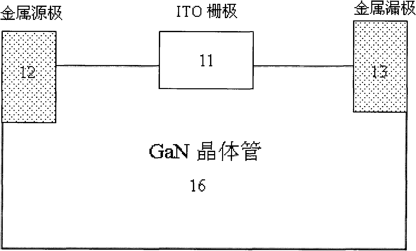
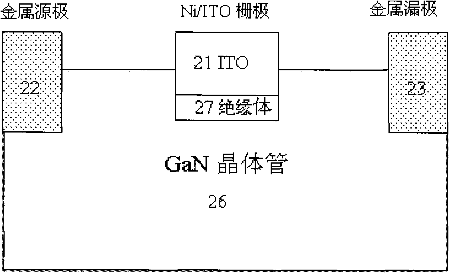
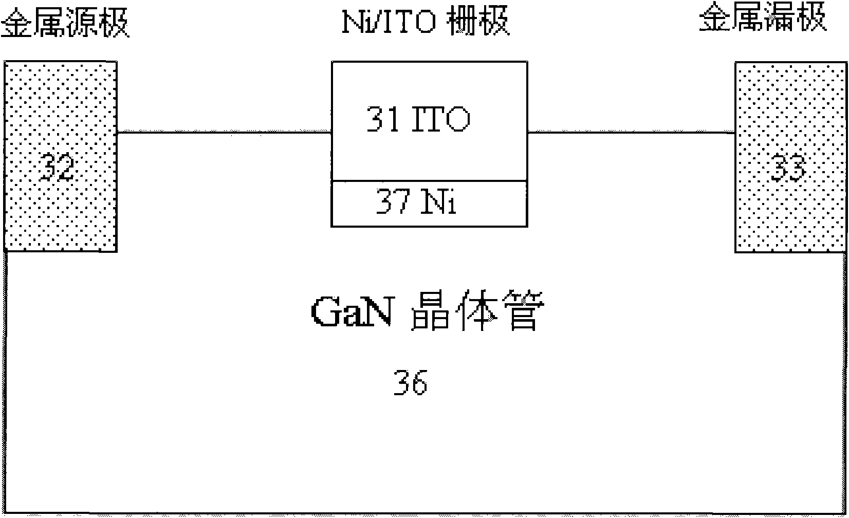
[0041] The present invention proposes a new electrode design. Based on this electrode design, the device can be various forms of transistors, especially transparent GaN field effect transistors. The type of transistor can be one or more of the following, but not limited to: ① high electron mobility transistor, heterojunction insulated gate field effect transistor (HFET); ② metal-oxide-semiconductor field effect transistor (MOSFET) or Metal-insulating layer-semiconductor field effect transistor (MISFET); ③Bipolar junction transistor (BJT); ④Other transistors, such as JFET, IGBT, MESFET, etc.

[0042] Transistor materials can be one or more of the following, but not limited to: ①Gallium electrode AlxGayIn1-x-yN; ②Nitrogen electrode AlxGayIn1-x-yN; ③Gallium electrode and nitrogen electrode mixture; ④GaN and other materials Combinations, such as a combination of GaN and GaAs.

[0043...


PUM


Abstract

The invention provides a transparent electrode realization scheme. The electrode structure is in favor of the increase of transmittance of an electrode and the effective identification of failure mechanism of a transistor by optical methods, such as electroluminescence and the like. The method is also in favor of the application of a device in the display field.

Description

Technical field [0001] Field-effect transistors based on wide-gap semiconductor gallium nitride (GaN) have good prospects in the application of radio frequency and power devices. The present invention proposes a new electrode design and production plan, which is beneficial to more intuitively analyze the reliability of the device. At the same time, transparent electrode gallium nitride devices can also be applied in the display field. Background technique [0002] The dielectric breakdown electric field of the third-generation semiconductor gallium nitride (GaN) is much higher than that of the first-generation semiconductor silicon (Si) or the second-generation semiconductor gallium arsenide (GaAs), up to 3MV / cm, which makes its electronic devices able to withstand Very high voltage. At the same time, gallium nitride can form a heterojunction structure with other gallium compound valence semiconductors (III-N). Because III-N semiconductors have strong spontaneous polarization ...

Claims


Application Information

Patent Timeline
Patent Type & Authority Applications(China)
IPC IPC(8): H01L29/43H01L21/28
Inventor 范爱民
Owner 西安能讯微电子有限公司
Why Eureka
Try Eureka