Semiconductor contact tetrode charge number density difference type thermoelectric conversion device

A thermoelectric conversion device and semiconductor technology, which can be applied to thermoelectric devices, circuits, electrical components, etc., and can solve problems such as charge number density and differential thermoelectric conversion devices that have not yet been seen.

Inactive Publication Date: 2010-11-17
冯建明
View PDF0 Cites 6 Cited by
  • Summary
  • Abstract
  • Description
  • Claims
  • Application Information

AI Technical Summary

Problems solved by technology

[0002] At present, only thermoelectric conversion devices that utilize the thermoelectric electromotive force in the semiconductor contact circuit can be seen on the market, and no thermoelectric conversion device that utilizes the charge number density difference between the same semiconductor in the semiconductor contact circuit has been seen.

Method used


Image

  • Semiconductor contact tetrode charge number density difference type thermoelectric conversion device
  • Semiconductor contact tetrode charge number density difference type thermoelectric conversion device
  • Semiconductor contact tetrode charge number density difference type thermoelectric conversion device

Examples


Embodiment Construction

[0019] Below in conjunction with accompanying drawing and specific embodiment the present invention is described in further detail:

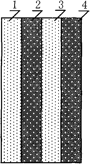
[0020] figure 1 Among them, the right surface of the N-type semiconductor plate 1 is in contact with the left surface of the P-type semiconductor plate 2, the right surface of the P-type semiconductor plate 2 is in contact with the left surface of the N-type semiconductor plate 3, and the N-type semiconductor plate 3 is in contact with the left surface. The right surface is in contact with the left surface of the P-type semiconductor plate 4 .

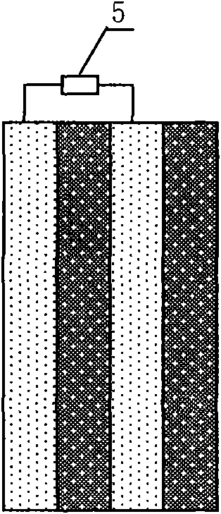
[0021] figure 2 In the shown embodiment, the load 5 is connected between the N-type semiconductor plate 1 and the N-type semiconductor plate 3 by wires, so that the load 5 can output electric energy and convert heat energy into electric energy.

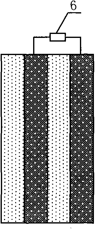
[0022] image 3 In the shown embodiment, the load 6 is connected between the P-type semiconductor plate 2 and the P-type semiconductor plate 4 by wires, so ...


PUM


Abstract

The invention discloses a thermoelectric conversion device which operates by using the charge number density difference between semiconductors of the same type in a semiconductor contact return circuit. The thermoelectric conversion device comprises two N-type semiconductor boards and two P-type semiconductor boards, the right surface of the N-type semiconductor board 1 is in contact with the left surface of the P-type semiconductor board 2, the right surface of the P-type semiconductor board 2 is in contact with the left surface of the N-type semiconductor board 3, and the right surface of the N-type semiconductor board 3 is in contact with the left surface of the P-type semiconductor board 4. A load is applied between the N-type semiconductor board 1 and the N-type semiconductor board 3, or a load is applied between the P-type semiconductor board 2 and the P-type semiconductor board 4. The load contains electric energy output, and thermal energy is converted into electric energy.

Description

technical field [0001] The present invention relates to thermoelectric conversion devices, and more particularly, the present invention relates to thermoelectric conversion devices that operate by exploiting charge number density differences between the same semiconductors in a semiconductor contact circuit. Background technique [0002] At present, only thermoelectric conversion devices that utilize the thermoelectric electromotive force in the semiconductor contact circuit can be seen on the market, and no thermoelectric conversion device that utilizes the charge number density difference between the same semiconductors in the semiconductor contact circuit has been seen. Contents of the invention [0003] The object of the present invention is to provide a thermoelectric conversion device with simple structure. [0004] The technical scheme of the present invention is: two N-type semiconductor plates and two P-type semiconductor plates are in contact with each other, and...

Claims


Application Information

Patent Timeline
Patent Type & Authority Applications(China)
IPC IPC(8): H01L37/00
Inventor 冯建明
Owner 冯建明
Why Eureka
Try Eureka