Photomultiplier tube
A photomultiplier tube and electron multiplication technology, applied in electron multiplier tubes, discharge tubes, multiplier electrodes, etc., can solve the problems of reduced withstand voltage and incident insulating substrates.
- Summary
- Abstract
- Description
- Claims
- Application Information
AI Technical Summary
Problems solved by technology
Method used
Image
Examples
Embodiment Construction
[0021] Hereinafter, preferred embodiments of the photomultiplier tube according to the present invention will be described in detail with reference to the drawings. However, in the description of the drawings, the same reference numerals are assigned to the same or corresponding parts, and overlapping descriptions are omitted.
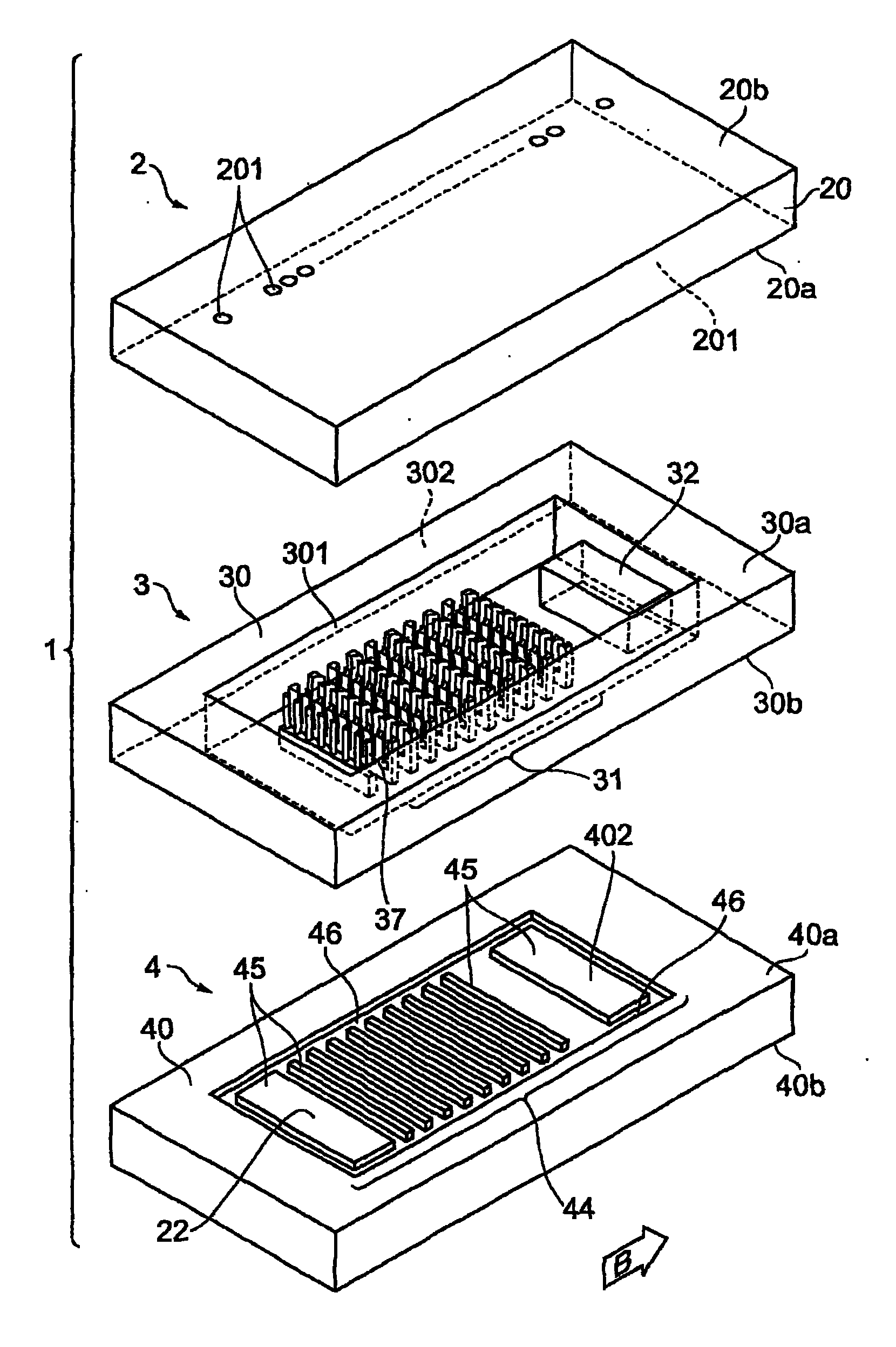
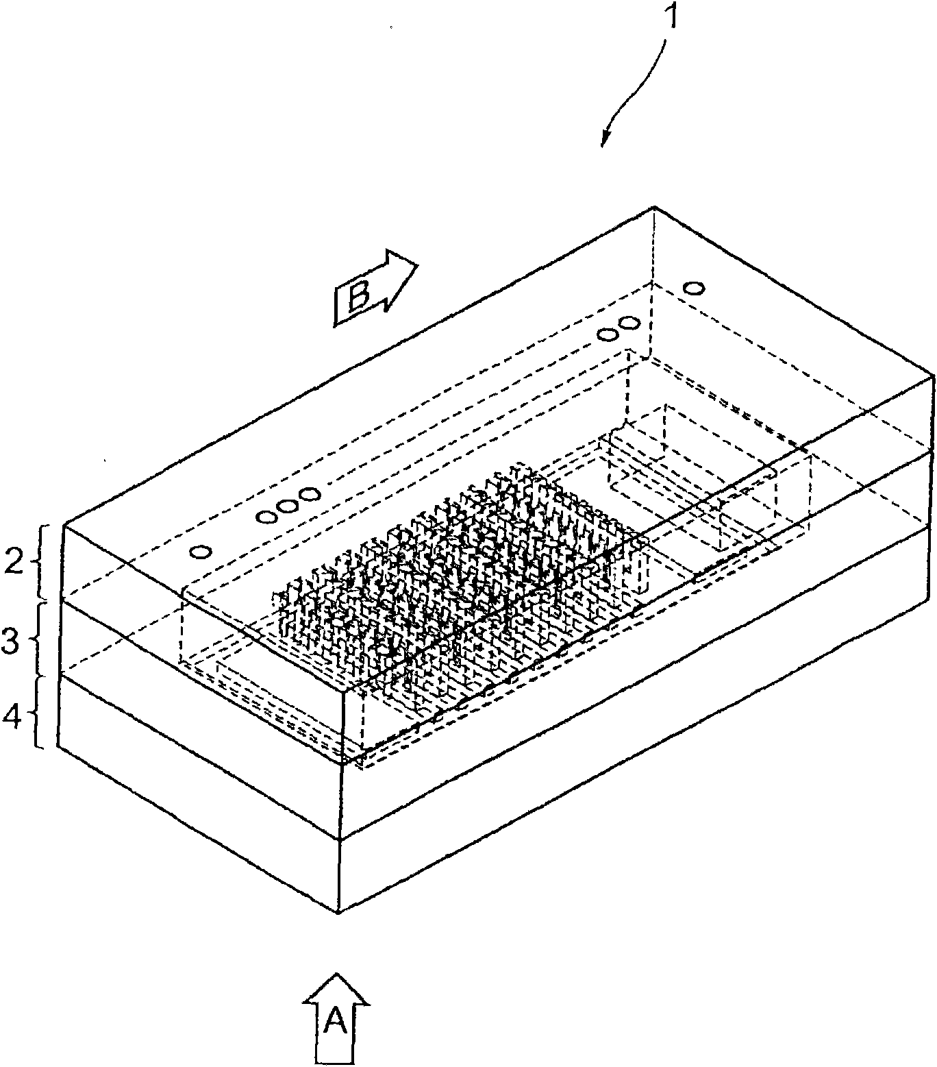
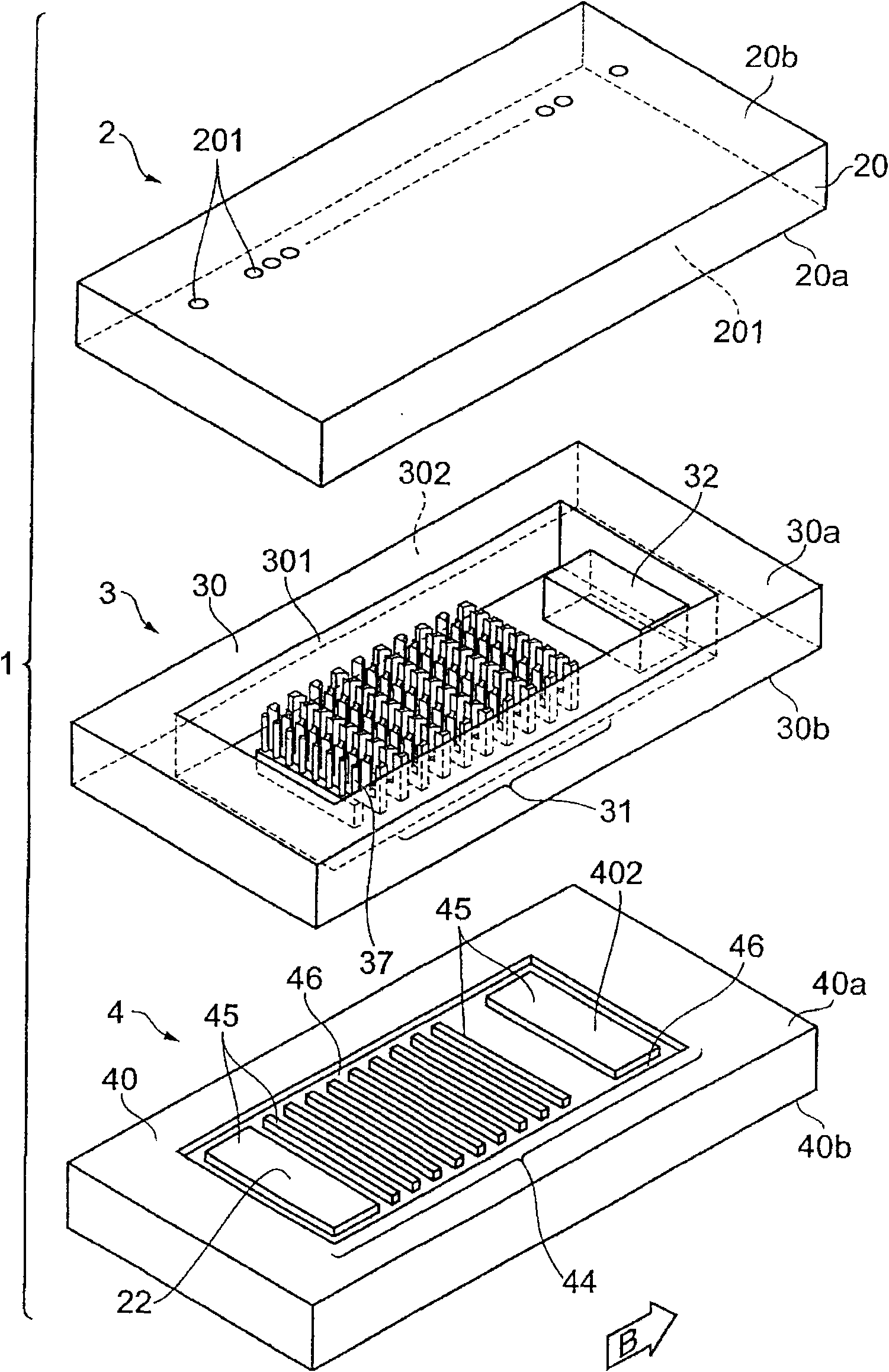
[0022] FIG. 1 is a perspective view of a photomultiplier tube 1 according to a preferred embodiment of the present invention, and FIG. 2 is an exploded perspective view of the photomultiplier tube 1 of FIG. 1 .
[0023] The photomultiplier tube 1 shown in FIG. 1 is a photomultiplier tube with a transmissive photoelectric surface, and is composed of an upper frame 2 (glass substrate), a side wall frame 3 (silicon substrate), and a lower frame 4 (glass substrate). of the box. This photomultiplier tube 1 is an electron tube, wherein, the direction in which light is incident on the photoelectric surface intersects the multiplication direction of electrons...
PUM
 Abstract
Description
Claims
Application Information
 - R&D
- Intellectual Property
- Life Sciences
- Materials
- Tech Scout
- Unparalleled Data Quality
- Higher Quality Content
- 60% Fewer Hallucinations
Browse by: Latest US Patents, China's latest patents, Technical Efficacy Thesaurus, Application Domain, Technology Topic, Popular Technical Reports.
© 2025 PatSnap. All rights reserved.Legal|Privacy policy|Modern Slavery Act Transparency Statement|Sitemap|About US| Contact US: help@patsnap.com


