Liquid crystal display device and manufacture method thereof
A liquid crystal display and device technology, applied in the field of liquid crystal displays, can solve the problems affecting the brightness and contrast of the display screen, the decrease of the light transmittance of the liquid crystal panel, and the reduction of the clarity of the display screen.
Inactive Publication Date: 2010-08-25
BOE TECH GRP CO LTD +1
View PDF0 Cites 4 Cited by
- Summary
- Abstract
- Description
- Claims
- Application Information
AI Technical Summary
Problems solved by technology
However, in the specific use process, the inventor found that attaching a film with touch function on the liquid crystal panel will reduce the light transmittance of the liquid crystal panel, which will affect the technical indicators such as brightness and contrast of the display screen, and will also reduce the display screen. clarity of
Method used
View moreImage
Smart ImageViewing Examples

Examples
Embodiment 1
Embodiment 2
Login to View More PUM
 Abstract
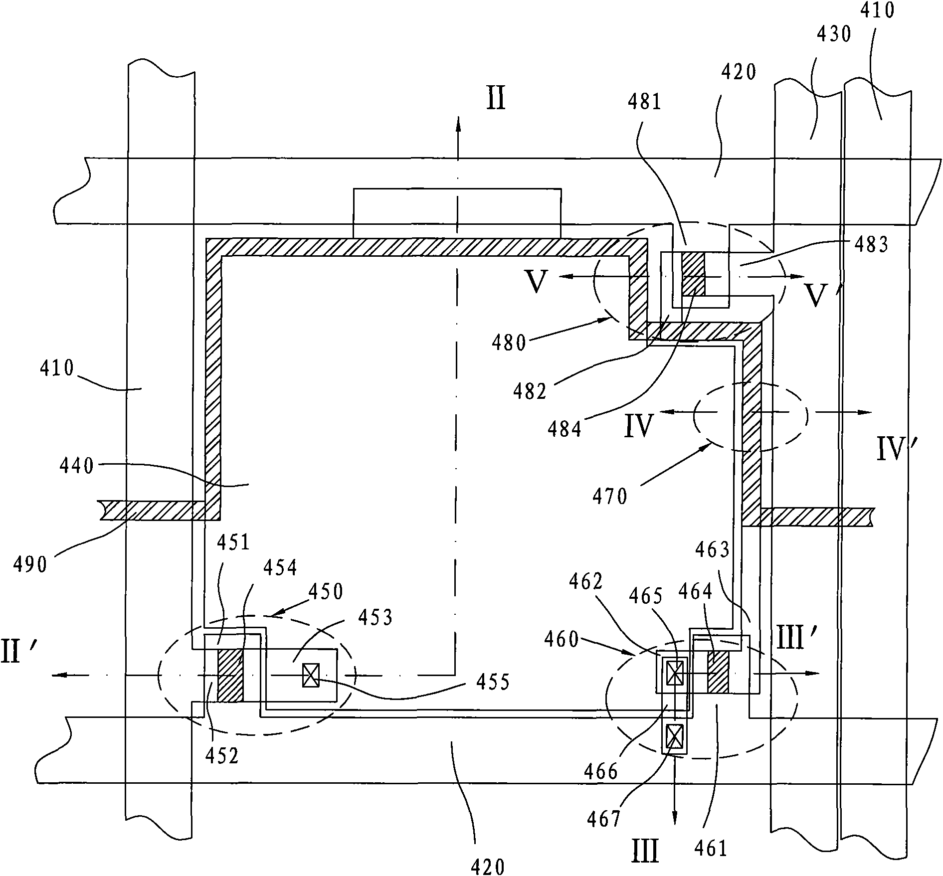
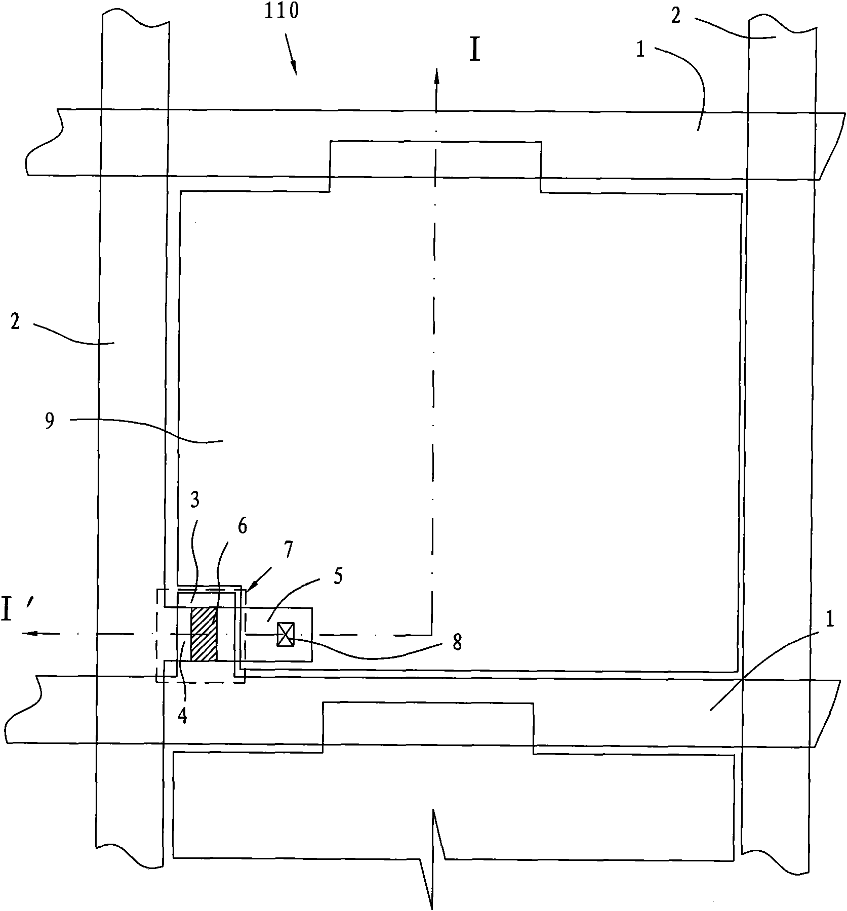
The invention discloses a liquid crystal display device and a manufacture method thereof, which relate to the field of liquid crystal displays and solve the problem that the traditional liquid crystal display devices with touch functions influence the brightness, the contrast and the definition of display frames. In the embodiment of the invention, a signal wire and a light-induced thin film transistor are additionally installed in the liquid crystal display device, and the light-induced thin film transistor is provided with an auxiliary spacer which has the gap with the light-induced thin film transistor; the surface of the auxiliary spacer is provided with a reflection layer, wherein the the drain electrode of the light-induced thin film transistor needs to be input to the signal wire, whereas the grid electrode and the source electrode of the light-induced thin film transistor are respectively connected to a grid electrode scanning line. The liquid crystal display device and the manufacture method thereof are mainly used for the liquid crystal displays, in particular to the liquid crystal displays with the touch functions.
Description
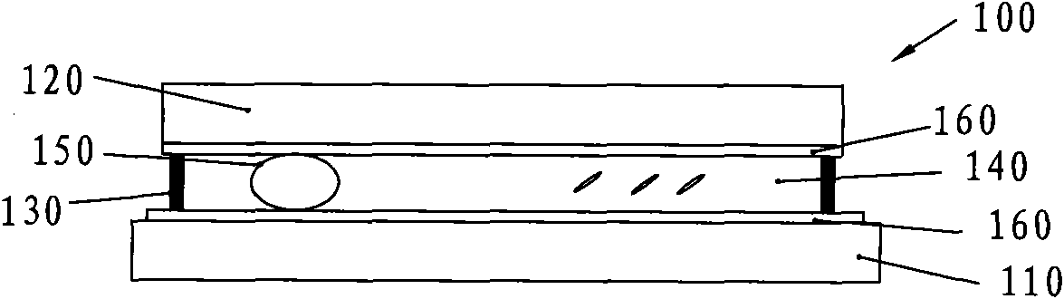
Liquid crystal display device and manufacturing method thereof technical field The invention relates to the field of liquid crystal displays, in particular to a liquid crystal display device in a liquid crystal display with touch function, and a manufacturing method of the liquid crystal display device. Background technique A liquid crystal display includes pixel units arranged in a matrix, and a driving circuit for driving the pixel units, and uses an electric field to control light transmittance of liquid crystals to display images. As shown in FIG. 1 , the liquid crystal display device 100 includes a thin film transistor (TFT, ThinFilmTransistor) array substrate 110 and a color filter glass substrate 120 facing each other, and the two substrates are sealed to the box by a sealant 130 to form the liquid crystal display device 100, And the TFT array substrate 110 and the color filter glass substrate 120 are coated with an alignment layer 160; the liquid crystal display de...
Claims
Login to View More Application Information
Patent Timeline
 IPC IPC(8): G02F1/1362H01L27/12H01L21/84
Inventor 王峥黄应龙
Owner BOE TECH GRP CO LTD
Features
- R&D
- Intellectual Property
- Life Sciences
- Materials
- Tech Scout
- Unparalleled Data Quality
- Higher Quality Content
- 60% Fewer Hallucinations
Learn More Browse by: Latest US Patents, China's latest patents, Technical Efficacy Thesaurus, Application Domain, Technology Topic, Popular Technical Reports.
© 2025 PatSnap. All rights reserved.Legal|Privacy policy|Modern Slavery Act Transparency Statement|Sitemap|About US| Contact US: help@patsnap.com