
Integrated circuit

A technology of integrated circuits and metal layers, applied in circuits, electrical components, electrical solid devices, etc., can solve problems such as occurrence

Active Publication Date: 2010-06-16
MEDIATEK INC
View PDF0 Cites 0 Cited by
  • Summary
  • Abstract
  • Description
  • Claims
  • Application Information

AI Technical Summary

Problems solved by technology

Also, if the pad spacing is reduced (connection pads are located closer to each other), electromigration issues are likely to occur

Method used


Image

  • Integrated circuit
  • Integrated circuit
  • Integrated circuit

Examples


Embodiment Construction

[0014] Certain terms are used in the description and claims to refer to particular elements. Those skilled in the art should understand that hardware manufacturers may use different terms to refer to the same component. The specification and claims do not use the difference in name as a way to distinguish components, but use the difference in function of components as a criterion for distinguishing. "Include" mentioned throughout the description and claims is an open-ended term, so it should be interpreted as "including but not limited to". In addition, the term "coupled" herein includes any direct and indirect means of electrical connection. Therefore, if it is described that the first device is coupled to the second device, it means that the first device may be directly electrically connected to the second device, or indirectly electrically connected to the second device through other devices or connection means.

[0015] One of the objects of the present invention is to p...


PUM


Abstract

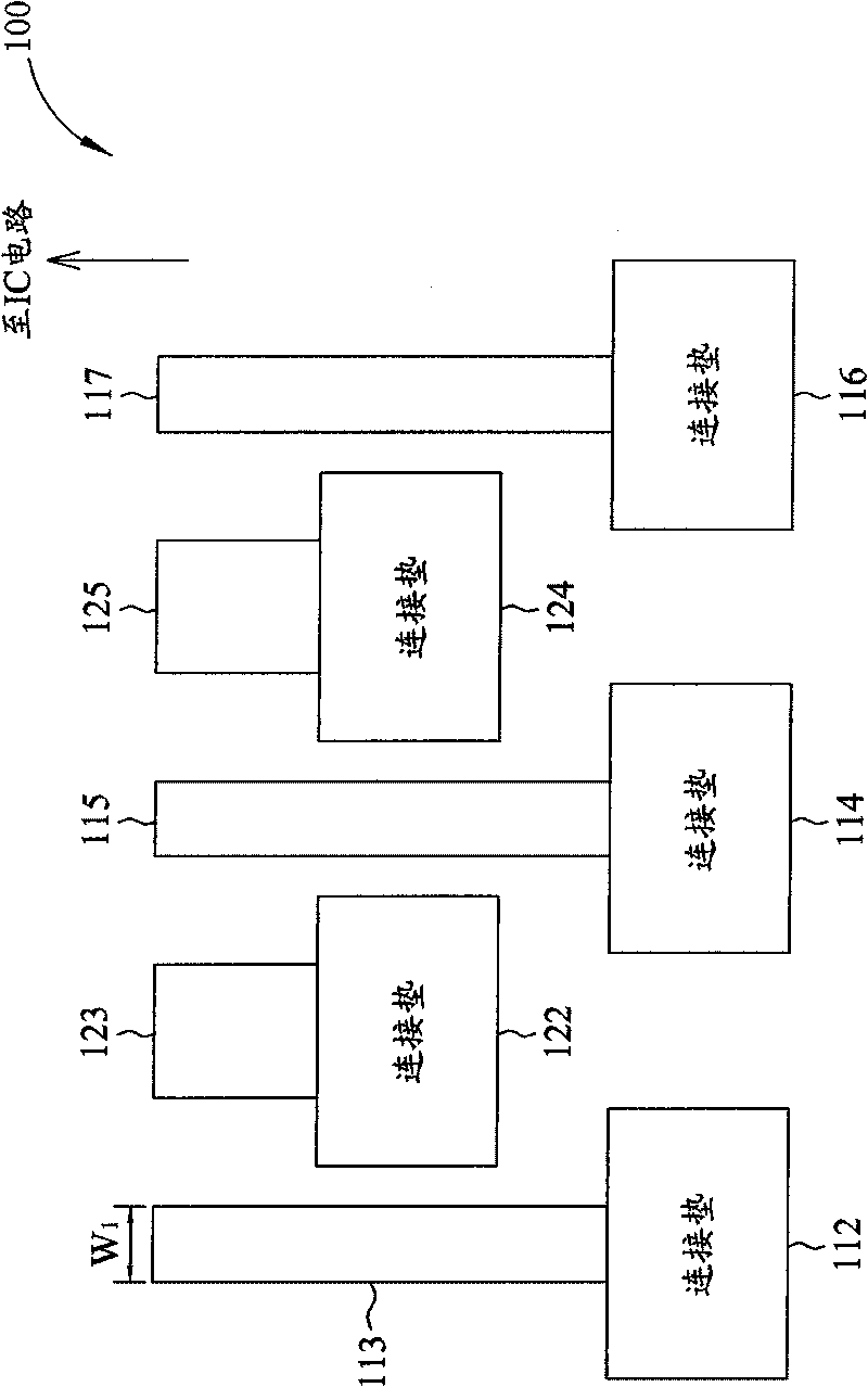
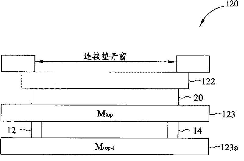
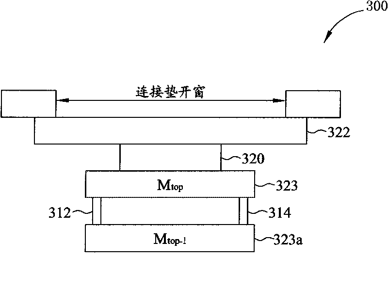
An integrated circuit includes: a substrate; and a bond pad array on the substrate. The bond pad array includes: a row of inner bond pads, each inner bond pad positioned with respect to a plurality of inner pad openings; a plurality of first inner metal layers respectively coupled to the inner bond pads for transmitting signals between the inner pads and an internal circuit, where at least one first inner metal layer has a width less than a width of a corresponding inner bond pad; a row of outer bond pads, staggered with respect to the row of inner bond pads; and a plurality of first outer metal layers respectively coupled to the outer bond pads for transmitting signals between the outer pads and the internal circuit, where at least one inner bond pad overlaps adjacent first outer metal layers. The integrated circuit can reduce the distance of the bond pads of integrated circuit chip and maintain good electromigration properties.

Description

technical field [0001] The present invention relates to a bond pad array for a complex integrated circuit, and more particularly to a bond pad array with small pitch and good electro-migration characteristics pad array. Background technique [0002] An integrated circuit (Integrated Circuit, hereinafter referred to as IC) chip uses metal connection pads to receive signals from other circuits and provide signals to other circuits. The connection pad is composed of a plurality of metal layers, which are generally rectangular, and some of the metal layers can also be used to transmit signals between the connection pad and other circuits of the IC chip. Conductive lines formed from one or more metal layers connect the connection pads to the circuit. [0003] For a chip, the size of the connection pads is relatively large, so the arrangement of the connection pads limits the remaining space of the circuit. Connection pads are usually arranged around the edge of the IC chip. T...

Claims


Application Information

Patent Timeline
IPC IPC(8): H01L23/485H01L23/528H01L23/525
CPCH01L2224/05093H01L2224/06153H01L2924/01082H01L2924/00014H01L2224/85399H01L24/05H01L2224/45099H01L24/06H01L2924/14H01L2924/01033H01L2224/05599H01L2224/02166H01L2924/01014H01L2224/023H01L2224/05553H01L2924/0001
Inventor 萧全成李洪松林奕成饶哲源
Owner MEDIATEK INC
Learn More