Array tester

A technology of array test and fixed block, which is applied in the direction of measuring device, electronic circuit test, measuring electricity, etc., can solve the problems of prolonged test time and long stabilization time.

Inactive Publication Date: 2012-04-18
TOP ENG CO LTD
View PDF1 Cites 0 Cited by
  • Summary
  • Abstract
  • Description
  • Claims
  • Application Information

AI Technical Summary

Problems solved by technology

[0010] Therefore, the stabilization time from when the modulation block reaches above the substrate to be tested to when the modulation block stops completely is too long, resulting in extended test time
[0011] In addition, when testing a large-sized substrate, the modulation block must move more times than in a small-sized substrate, and in this case, the extension of the test time due to this increase in the stabilization time becomes more severe. for serious

Method used


Image

  • Array tester
  • Array tester
  • Array tester

Examples


Embodiment Construction

[0022] The present invention will be described more fully hereinafter with reference to the accompanying drawings that illustrate exemplary embodiments of the invention. This invention may, however, be embodied in many different forms and should not be construed as limited to the exemplary embodiments set forth herein. Rather, these exemplary embodiments are provided so that this disclosure will be thorough and will fully convey the scope of the invention to those skilled in the art. In the drawings, the size and relative sizes of layers and regions may be exaggerated for clarity. The same reference numerals in the figures denote the same elements.

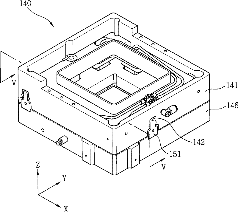
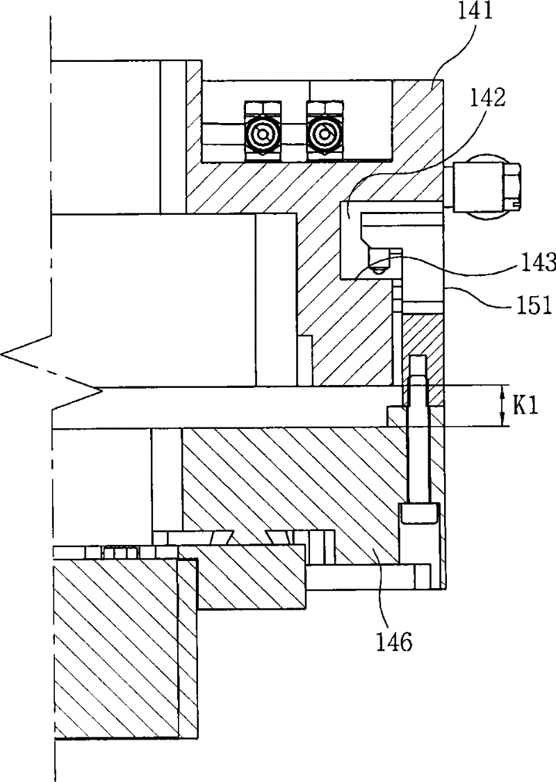
[0023] figure 1 is a perspective view of an array testing apparatus 100 for detecting electrical defects of electrodes formed on a substrate 10 according to an embodiment.

[0024] The substrate 10 may be a panel included in a flat display panel. For example, the substrate 10 is a TFT panel of a thin film transistor liquid cry...


PUM


Abstract

The present invention provides an array tester. Fixed blocks moves parallelly along at least a direction. Modulating blocks conjoined to the lower part of the fixed blocks in a lifting manner and electrodes formed on a substrate form an electric field and detect defect of the substrate according to electric intensity. Air bearings are inserted between the fixed blocks and the modulating blocks and are used to prevent the modulating blocks from vibrating when the modulating blocks move. The center of a spraying stream of the air bearings is located at a height position of the modulating blockswhen the modulating blocks are conjoined to the fixed blocks, thereby, the vibration is reduced when the modulating blocks move. Furthermore, a stable time is shortened, thus, it is possible to perform array test at a high speed.

Description

[0001] Related Application Cross Reference [0002] This application claims priority from Korean Patent Application No. 10-2008-0097723 filed on October 6, 2008, the disclosure of which is hereby incorporated by reference in its entirety. technical field [0003] The present invention relates to an array testing device for detecting electrical defects of electrodes formed on a substrate. Background technique [0004] Electro-optical devices for receiving electric power and emitting light include flat panel displays such as liquid crystal displays (LCDs), plasma display panels (PDPs), and the like. [0005] Generally, an electro-optical device includes a substrate on which a plurality of electrodes are formed. For example, a thin film transistor (TFT) LCD substrate includes: a TFT substrate; a color substrate on which a color filter and a common electrode are formed and opposite to the TFT substrate; a liquid crystal injected between the TFT substrate and the color substrate...

Claims


Application Information

Patent Timeline
Patent Type & Authority Patents(China)
IPC IPC(8): G02F1/1362G02F1/13G01R31/00G01R31/28G01R29/08
CPCG01R31/2853G01R31/2856G01R31/2867G01R31/2879
Inventor 潘俊浩张文柱
Owner TOP ENG CO LTD
Why Eureka
Try Eureka