Lateral diffusion metal oxide semiconductor transistor structure

A technology of oxide semiconductors and transistors, applied in semiconductor devices, electrical components, circuits, etc., can solve problems such as low turn-on voltage, transistor failure, and low turn-on voltage

Inactive Publication Date: 2010-05-12
GRACE SEMICON MFG CORP
View PDF1 Cites 2 Cited by
  • Summary
  • Abstract
  • Description
  • Claims
  • Application Information

AI Technical Summary

Problems solved by technology

[0006] In the above mechanism, the thinner part of the oxide layer GOX is an effective conductive part, and because this part of the oxide layer GOX is relatively thin, there are fewer ions that can move in the STI and P-type drift region P-d below it, so this part The turn-on voltage that the region can withstand is lower, which in turn causes the LDNMOS to have a lower turn-on voltage, which is lower than the normal turn-on voltage of the transistor, thus forming two bumps on the Id-Vg curve of the transistor (such as Figure 4 The dotted curve in the middle), that is, the transistor has a bimodal effect, and its performance is that in the subcritical region (B-threshold), when the MOS is not turned on (Vg
The early appearance of this leakage will directly lead to the failure of the transistor and the low yield of the product

Method used


Image

  • Lateral diffusion metal oxide semiconductor transistor structure
  • Lateral diffusion metal oxide semiconductor transistor structure
  • Lateral diffusion metal oxide semiconductor transistor structure

Examples


Embodiment Construction

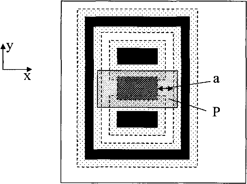
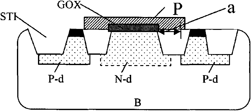
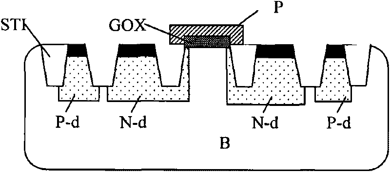
[0022] In order to better understand the technical content of the present invention, specific embodiments are given together with the attached drawings for description as follows.

[0023] Figure 4 It is a schematic top view of the LDNMOS structure disclosed in the present invention; Figure 5 for Figure 4 Schematic cross-sectional view of the LDNMOS structure along the x direction; Image 6 for Figure 4 A schematic cross-sectional view of the LDNMOS structure along the y direction.

[0024] Please also refer to Figure 4~6 In this embodiment, the LDNMOS structure includes a base layer B, an oxide layer GOX, and a polysilicon layer P in order from bottom to top.

[0025] In this embodiment, the base layer B is an N well, and the polysilicon layer P formed thereon serves as the gate G of the LDNMOS. On both sides of the oxide layer GOX in the base layer B, there are corresponding N-type drift regions N-d as the source S and drain D of the LDNMOS.

[0026] The N-type d...


PUM


Abstract

The invention provides a lateral diffusion metal oxide semiconductor transistor (LDNMOS) structure, comprising a substrate layer, an oxidation layer and a polysilicon layer which are distributed from bottom to top, wherein the polysilicon layer is used as a grid electrode of the LDNMOS. Two N type drift regions are respectively positioned at the two sides of the oxidation layer in the substrate layer and respectively used as a source electrode and a drain electrode of the LDNMOS. A P type drift region is annually arranged outside the grid electrode, the source electrode and the drain electrode in the substrate layer and as a base electrode of the LDNMOS. The annular P type drift region extends towards the other two sides of the oxidation layer between the source electrode and the drain electrode to a position which is 0-0.2 micrometer from the edge of the oxidation layer. The LDNMOS structure provided by the invention ensures that a thinner part in GOX of a grid oxidation layer of the LDNMOS can be compensated by the P type ions in the P type drift region, and the threshold voltage Vt of an apparatus is kept to be constant so that the double-hump effect of the LDNMOS is limited.

Description

technical field [0001] The invention relates to a structure of a laterally diffused metal oxide semiconductor transistor, and further relates to a structure of a laterally diffused metal oxide semiconductor transistor which avoids the double peak effect. Background technique [0002] Laterally Diffused N type Metal Oxide Semiconductor (LDNMOS) plays an important role in the design and manufacture of integrated circuits. For example, a laterally diffused metal oxide semiconductor transistor (HV LDNMOS) is widely used in a driver chip of a thin film transistor liquid crystal display. [0003] The structure diagram of the current LDNMOS is as follows figure 1 with figure 2 as shown, figure 1 is a schematic top view of a known LDNMOS structure; figure 2 for figure 1 Schematic diagram of the cross-section of the LDNMOS along the x direction; image 3 for figure 1 Schematic diagram of the cross-section of the LDNMOS along the y direction. The LDNMOS includes a base layer...

Claims


Application Information

Patent Timeline
Patent Type & Authority Applications(China)
IPC IPC(8): H01L29/78
Inventor 刘龙平令海阳陈爱军
Owner GRACE SEMICON MFG CORP
Why Eureka
Try Eureka