Defect detection system of panel component

A technology for defect detection and components, applied in measuring devices, material analysis through optical means, instruments, etc., can solve problems such as light intensity attenuation, energy consumption, production costs, light box thickness and bulky volume, etc.

Inactive Publication Date: 2011-04-13
IND TECH RES INST
View PDF4 Cites 0 Cited by
  • Summary
  • Abstract
  • Description
  • Claims
  • Application Information

AI Technical Summary

Problems solved by technology

[0005] The disadvantage of the light box made of fluorescent tubes is that the light box is thick and bulky, and a translucent diffuser and reflection mechanism are required to make the light uniform on the plane
However, the use of a diffuser design will attenuate the light intensity, so the fluorescent tube must increase the brightness to compensate, which consumes more energy and increases the production cost of the user.
In addition, due to the physical characteristics of fluorescent lamps, the light intensity can only be adjusted in multiple stages, and the light color produced is limited to the range of white light and daylight, and the adjustment range is limited.

Method used


Image

  • Defect detection system of panel component
  • Defect detection system of panel component
  • Defect detection system of panel component

Examples


Embodiment Construction

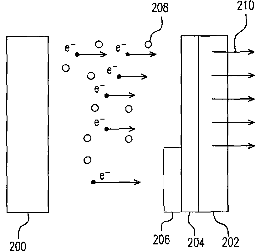
[0034] For example, the present invention can be applied to the product inspection planar light source equipment required on the production line. For the light source part of the detection light box, the present invention proposes an electron emission type flat light source (Flat electron emission lamp, FEEL) as the detection light source. Here, the planar light source refers to a planar light source, which can be a curved surface or a planar surface as required.

[0035] The light source of the detection light box is changed to an electron-emitting planar light source. Because it is a planar light source, there is no need to use a diffuser, which can reduce light loss. In addition, the light source device of the present invention can be manufactured into light sources of different sizes and shapes as required, for example, rectangular or circular as shown in FIG. 8 . The reflective mechanism only needs a flat reflective surface, and the overall detection equipment can be thi...


PUM


Abstract

The invention discloses a defect detection system of a component, which comprises a component to be detected, a platform carrying the component to be detected, a power supply unit and a light source device, wherein the light source device is controlled by the power supply unit to supply detection light to the component to be detected for defect detection; the light source device comprises a cathode structure, an anode structure, a fluorescent layer and a low-pressure gas layer; the fluorescent layer is positioned between the cathode structure and the anode structure; and the low-pressure gas layer is filled between the cathode structure and the anode structure, has the function of inducing the cathode structure to uniformly emit electrons, wherein the air pressure of the low-pressure gas layer is at the range of 0.1-10-3 torr, and the low-pressure gas layer is provided with an electron mean free path where at least enough number of electrons are allowed to directly collide with the fluorescent layer at operating voltage.

Description

technical field [0001] The present invention relates to a component defect detection system, such as detecting optically observable defects on panel components. Background technique [0002] Component defect detection can reduce a necessary process that leads to performance defects in the final product. For example, the components of the display panel or the transparent components may have defects on the surface or inside during the manufacturing process. This defect is also, for example, defects such as foreign matter particles adhering to the surface or surface cracks, or defects such as internal foreign matter particles, holes or cracks, etc., which are detected by various light inspections, such as pinholes, foreign matter or white spots, etc. and other defects. These defects can be detected by light passing through the component or reflected by the component surface. [0003] Figure 1A and Figure 1B A schematic diagram of a conventional component detection mechani...

Claims


Application Information

Patent Timeline
Patent Type & Authority Patents(China)
IPC IPC(8): G01N21/892
Inventor 李中裕陈世溥林依萍卓连益
Owner IND TECH RES INST
Why Eureka
Try Eureka