Output amplifier circuit, output circuit, data driver and display device
A technology of amplifying circuits and circuits, applied in the direction of coupling substation interface circuits, instruments, static indicators, etc., can solve the problems of output delay, noise, etc.
- Summary
- Abstract
- Description
- Claims
- Application Information
AI Technical Summary
Problems solved by technology
Method used
Image
Examples
Embodiment 1
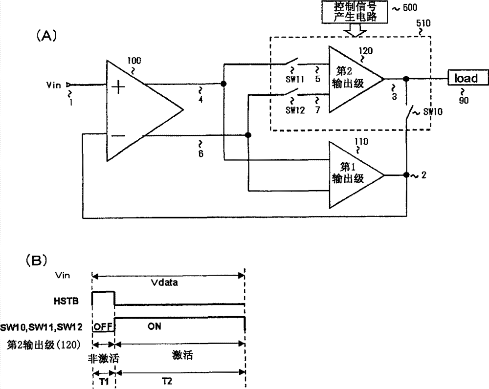
[0100] figure 1 is a diagram showing the configuration of an example of an output amplifier circuit according to the present invention. refer to figure 1 , in this example, with:
[0101] Differential stage 100;
[0102] 1st output stage 110;
[0103] 2nd output stage 120;
[0104] Switches SW11 and SW12 are respectively connected between the first and second outputs 4 and 6 of the differential stage 100 and the first and second input terminals 5 and 7 of the second output stage 120;
[0105] a switch SW10 connected between the output node 2 of the first output stage 110 and the output node 3 of the second output stage 120; and
[0106] Control signal generating circuit 500 .
[0107] Also, the differential stage 110 includes at least a differential pair and a load circuit. And in an output amplifier circuit with an intermediate stage, the differential stage 100 also includes the intermediate stage.
[0108] The output node 2 of the first output stage 110 is connecte...
Embodiment 2
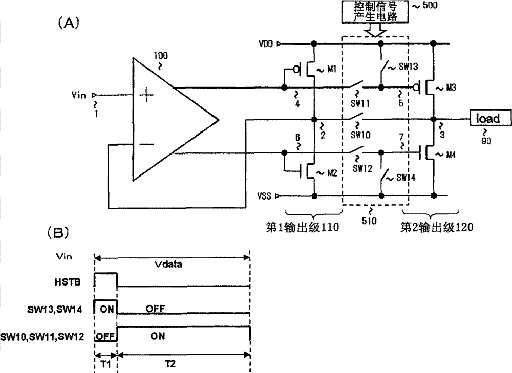
[0118] figure 2 (A) means figure 1A diagram of an example of a specific structure of the first and second output stages 110 and 120 of the . The first output stage 110 has: a pMOS transistor M1, the source of which is connected to the first power supply terminal (VDD) supplying the power supply voltage VDD, the gate connected to the first output 4 of the differential stage 100, and the drain connected to the output node 2; The source of the nMOS transistor M2 is connected to the second power supply terminal (VSS) that supplies the power supply voltage VSS, the gate is connected to the second output 6 of the differential stage 100 , and the drain is connected to the output node 2 . The second output stage 120 includes: a pMOS transistor M3 whose source is connected to the first power supply terminal, whose gate is connected to the first output 4 of the differential stage 100 via the switch SW11, and whose drain is connected to the output node 3; and an nMOS transistor M4, T...
Embodiment 3
[0129] image 3 (A) means figure 1 Figures of other examples of specific structures of the first and second output stages 110 and 120 of . refer to image 3 (A), this embodiment is composed of pMOS transistor M2C figure 2 The nMOS transistor M2 of the first output stage of (A), and the second output stage nMOS transistor M4 is constituted by the pMOS transistor M4C, between the gate 7 and the source (the output node 3 of the second output stage 120 ) of the pMOS transistor M4C Interconnect switch SW14C. Furthermore, in this embodiment, the structure of the differential stage 100 is such that when the voltage of the input voltage Vin changes, the first output 4 acts in a direction opposite to the voltage change of the input voltage Vin, and the second output of the differential stage 100 6 acts in the same direction as the voltage change of the input voltage Vin. The switching of other structures and switches is the same as the above-mentioned embodiment. In this embodi...
PUM
 Abstract
Description
Claims
Application Information
 - R&D
- Intellectual Property
- Life Sciences
- Materials
- Tech Scout
- Unparalleled Data Quality
- Higher Quality Content
- 60% Fewer Hallucinations
Browse by: Latest US Patents, China's latest patents, Technical Efficacy Thesaurus, Application Domain, Technology Topic, Popular Technical Reports.
© 2025 PatSnap. All rights reserved.Legal|Privacy policy|Modern Slavery Act Transparency Statement|Sitemap|About US| Contact US: help@patsnap.com


