
Efficacy push-pull buffer circuit, system and method for high frequency signals

A technology for buffering circuits and signals, applied in the direction of coupling/interface of logic circuits using field effect transistors, logic circuits, power reduction of field effect transistors, etc., capable of solving the obstacles of proper operation of source follower 400 and the limitation of buffer clock signals etc.

Inactive Publication Date: 2009-09-23
STMICROELECTRONICS SHANGHAI R&D
View PDF0 Cites 9 Cited by
  • Summary
  • Abstract
  • Description
  • Claims
  • Application Information

AI Technical Summary

Problems solved by technology

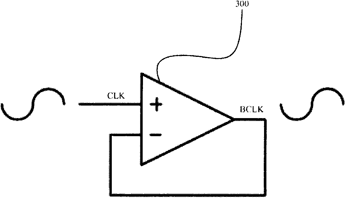
Using source follower 400, the voltage swing of the BCLK signal is limited by the gate-source voltage Vgs of NMOS transistor 402, and if the lowest level of the CLK signal is less than this gate-source voltage, the buffer clock signal is clipped
As the magnitude of the supply voltage Vdd decreases, the gate-source voltage Vgs of the NMOS transistor 402 becomes a significant impediment to the proper operation of the source follower 400

Method used


Image

  • Efficacy push-pull buffer circuit, system and method for high frequency signals
  • Efficacy push-pull buffer circuit, system and method for high frequency signals
  • Efficacy push-pull buffer circuit, system and method for high frequency signals

Examples


Embodiment Construction

[0017] 【17】 Figure 5 is a schematic diagram of a buffer circuit 500 according to an embodiment of the present invention, including a capacitor network 502 that receives an input signal VIN and generates bootstrap control signals VGN, VGP in response to the input signal to drive a push-pull stage 504 . In operation, in response to an input signal VIN, capacitive network 502 generates bootstrap control signals VBN and VBP, each having a magnitude that will be greater than supply voltage Vdd and less than reference voltage GND, thereby driving push-pull stage 504 to A buffered output signal BVOUT is generated that has a full-scale voltage swing from the supply voltage to the reference voltage, as will be explained in more detail below. Buffer circuit 500 consumes a relatively low amount of power while allowing buffered output signal BVOUT to have a full-scale voltage swing between supply voltage Vdd and reference voltage GND even for low supply voltages.

[0018] [18] In this s...


PUM


Abstract

The invention relates to an efficacy push-pull buffer circuit, a system and a method for high frequency signals. The buffer circuit comprises a biasing circuit which can be operated to generate a first bias signal and a second bias signal. A capacitance network comprises an input end suitable for receiving input signals and can be operated to respond to the input signal so as to generate a first bootstrapping signal and a second bootstrapping signal. A push-pull stage comprises a first control input end, a first control output end, a second control input end and a second control output end. The push-pull stage is coupled to the biasing circuit to receive the first and the second bias signals at the first and the second control input ends respectively, and is also coupled the capacitance network to receive the first and the second bootstrapping signals at the first and the second control output ends respectively. The push-pull stage can be operated to respond to the first and the second bootstrapping signals so as to generate buffer output signals at the output ends.

Description

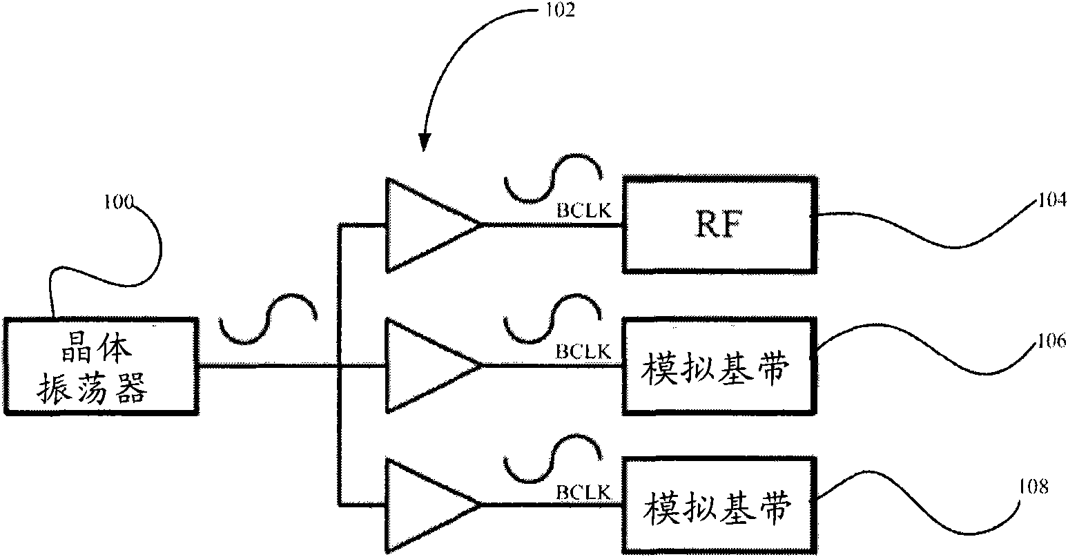
technical field [0001] [1] Embodiments of the present invention generally relate to buffer circuits, and more particularly, to push-pull buffer circuits, systems and methods for high frequency signals. technical background [0002] [2] Many electronic systems use high-frequency signals, such as clock signals, that must be supplied to a large number of components within the system. In these cases, buffer circuits are often required to adequately drive the large number of components that receive the clock signal and to isolate the circuit that generates the high-frequency clock signal, such as a crystal oscillator, from the large number of components. This isolation is necessary so that the circuits generating the high-frequency clock signal are not unduly loaded by these components, which would cause unwanted variations in the high-frequency clock signal, such as in the frequency, amplitude and phase of the clock signal changes in . [0003] 【3】 figure 1 shows a convention...

Claims


Application Information

Patent Timeline
Patent Type & Authority Applications(China)
IPC IPC(8): H03K19/0175H03K19/0185H03K19/018
CPCH03F2203/30081H03F2203/30114H03K19/0013H03F1/308H03F3/301H03F2200/18
Inventor 赵建华郜小茹
Owner STMICROELECTRONICS SHANGHAI R&D
Learn More