
A structure of liquid crystal display panel

A technology for liquid crystal display panels and substrates, which can be used in static indicators, nonlinear optics, optics, etc., and can solve the problems of insufficient liquid crystal filling, reduced scrap cost, and uneven chromaticity.

Inactive Publication Date: 2009-09-16
CPTF VISUAL DISPLAY (FUZHOU) LTD +1
View PDF0 Cites 2 Cited by
  • Summary
  • Abstract
  • Description
  • Claims
  • Application Information

AI Technical Summary

Problems solved by technology

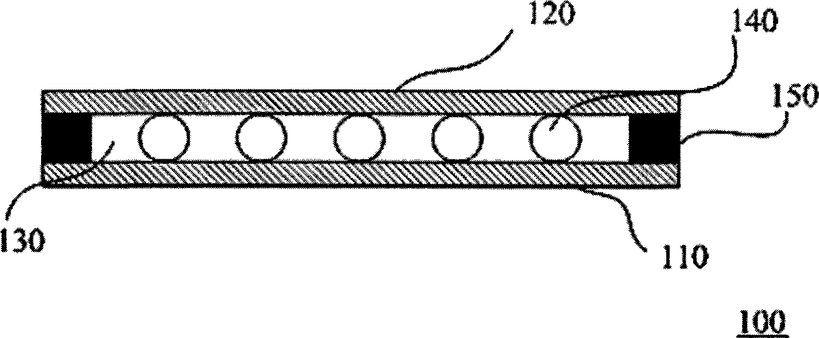
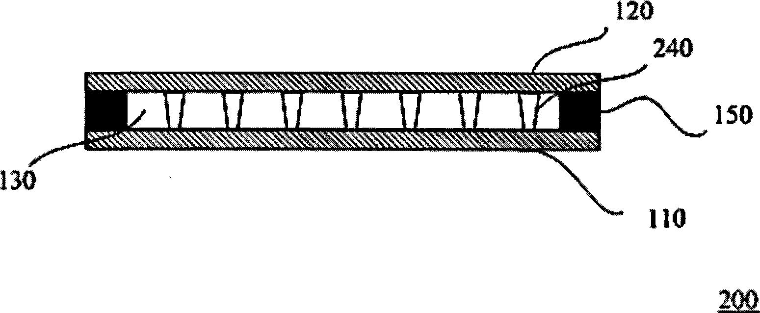
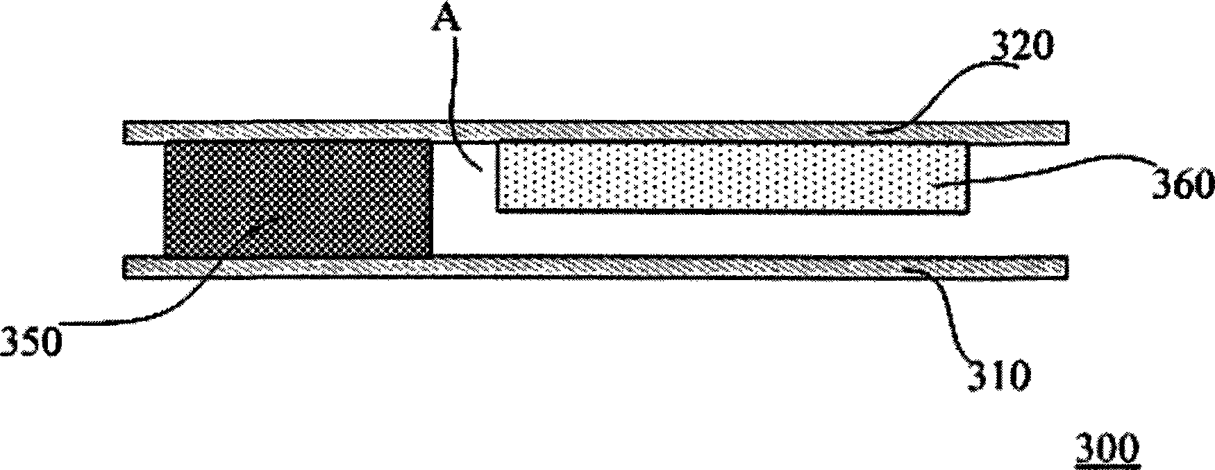
[0007] The object of the present invention is to provide a liquid crystal display panel structure, which can not only solve the problem of uneven chromaticity caused by insufficient liquid crystal filling, but also increase the margin of liquid crystal filling, and then Enable scrap costs to be effectively reduced

Method used


Image

  • A structure of liquid crystal display panel
  • A structure of liquid crystal display panel
  • A structure of liquid crystal display panel

Examples


Embodiment Construction

[0035] Figure 4 is a schematic cross-sectional view of a liquid crystal display panel according to a preferred embodiment of the present invention. Figure 5 It is a schematic partial top view of a color filter substrate according to a preferred embodiment of the present invention. Please also refer to Figure 4 and Figure 5 The liquid crystal display panel 400 in the best embodiment of the present invention includes a thin film transistor array substrate 410, a color filter substrate 420, a frame glue 450, a light shielding layer 460, and a thin film transistor array substrate 410 and a color filter substrate. A liquid crystal layer (not shown) between the substrates 420 . The liquid crystal layer is encapsulated in the thin film transistor array substrate 410 and the color filter substrate 420 by the sealant 450 .

[0036] The above-mentioned color filter substrate 420 includes a base 421 and a light-shielding layer 460 , a part of the light-shielding layer 460 is disp...


PUM


Abstract

The invention relates to a structure of liquid crystal display panel. The structure comprises a colour light filter base plate, an electric crystal array base plate and a liquid crystal layer. The colour light filter base plate includes a substrate and a light shielding layer. The surface of the light shielding layer around the substrate is provided with at least one sunken holding chamber. The liquid crystal layer is packed between the electric crystal array base plate and the colour light filter base plate by means of a frame. The structure of liquid crystal display panel can not only solve the problem of non-uniform chromaticity caused by insufficient liquid crystal filling amount, also enhance margin of the liquid crystal filling amount, so as to effectively reduce scrap cost.

Description

technical field [0001] The invention relates to a structure of a liquid crystal display panel. Background technique [0002] The rapid progress of the multimedia society is mostly due to the rapid progress of semiconductor devices or display devices. As far as the display panel is concerned, liquid crystal display (LCD) panels with superior characteristics such as high image quality, good space utilization efficiency, low power consumption, and no radiation have gradually become the mainstream of the market. [0003] Generally speaking, the three main process steps of a liquid crystal display panel (TFT-LCD) include: (1) thin film transistor (TFT) array substrate segment (Arrary) (2) panel assembly segment (Cell) (3) module packaging (Module Assembly). The manufacturing process in the thin film transistor array substrate section is very similar to the semiconductor manufacturing process. First, the alkali-free glass substrate must be cleaned, and then a multi-layer thin fi...

Claims


Application Information

Patent Timeline
IPC IPC(8): G02F1/133G02F1/1335
Inventor 余岱璟钟佳龙高振仁
Owner CPTF VISUAL DISPLAY (FUZHOU) LTD
Learn More