
Method for processing address discontinuity in MTD design of NAND flash memory

A technology of flash memory and address, which is applied in MTD design to deal with discontinuous addresses, and can solve problems such as NAND flash memory that cannot be adapted and does not support multi-planes

Active Publication Date: 2009-07-01
ANYKA (GUANGZHOU) MICROELECTRONICS TECH CO LTD
View PDF0 Cites 9 Cited by
  • Summary
  • Abstract
  • Description
  • Claims
  • Application Information

AI Technical Summary

Problems solved by technology

[0003] Since most SLCs are single-plane designs, many original MTD designs do not support multi-plane NAND flash memory
At the same time, due to the rapid update of the manufacturing process of MLC, various methods of dividing planes are still being updated, and the original MTD design cannot adapt to these new changes.

Method used


Image

  • Method for processing address discontinuity in MTD design of NAND flash memory
  • Method for processing address discontinuity in MTD design of NAND flash memory
  • Method for processing address discontinuity in MTD design of NAND flash memory

Examples


Embodiment Construction

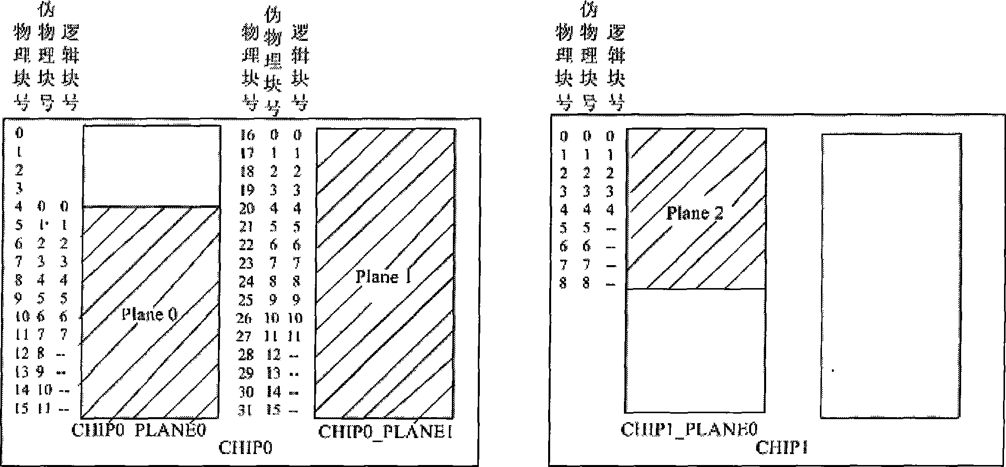
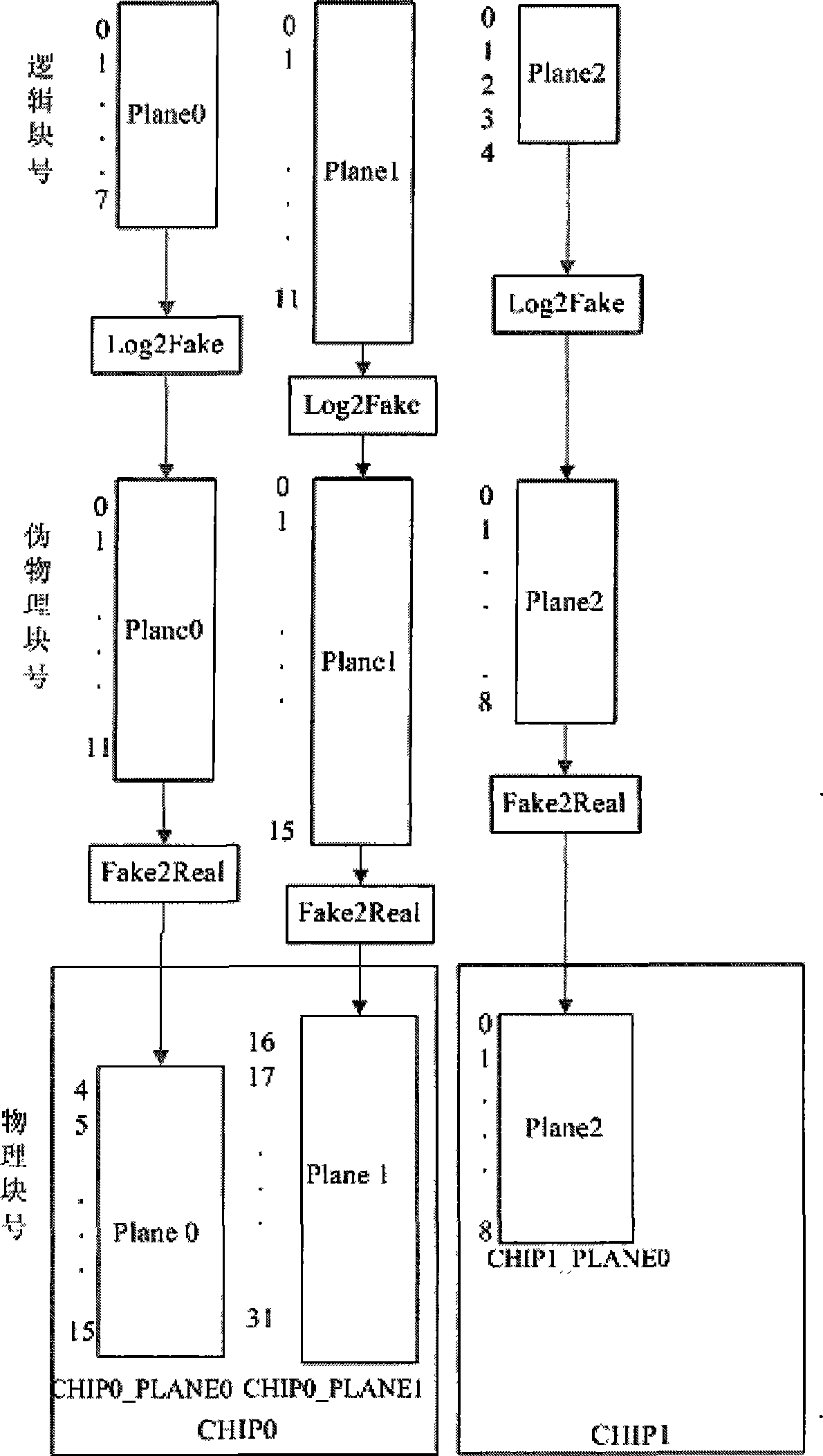
[0019] 1. According to the specific requirements of upper-layer applications such as storage content security requirements, the entire NAND flash memory space is divided into several different areas. One area may span multiple physical planes, or even multiple NAND flash memory chips. Each such divided area is managed by an MTD. The MTD needs to record the number of the physical plane where the first physical block of its management area is located and the offset of the physical block relative to the physical plane. figure 1 It is the division of two NAND flash memory chips, the front and rear addresses are divided into two physical planes, and the three logical planes Plane0, Plane1 and Plane2 are the area to be governed by an MTD. The three columns of numbers on the left side of the area are from left to right as shown in the figure, respectively representing the physical block number, pseudo-physical block number and logical block number. Each column of numbers is limited t...


PUM


Abstract

The invention discloses a method of unconsciously processing addresses in an MTD design which supports a multi-plane type NAND flash memory, which comprises dividing the whole NAND flash memory space into a plurality of regions, managing each region according to an MTD, abstracting each physical plane in each region into a logical plane, calculating the related logical block numbers by the MTD according to logical sector numbers transmitted from the upper application, then addressing according to the logical block numbers, corresponding the logical block numbers to false physical block number one by one through a mapping table, and finally realizing the access of MTD to a physical block number through related algorithm according to the false physical block numbers. The method facilitates the MTD to support an NAND flash memory comprising a plurality of physical planes, and to be independent from a changing MLC.

Description

technical field [0001] The invention relates to a method for dealing with address discontinuity in MTD design of NAND flash memory supporting multi-plane type. Background technique [0002] Various NAND flash memories have been widely used in mobile phones, digital and other terminal consumer products, and their capacity is getting larger and larger. Multi-plane MLC (Multi-Level Cell, multi-layer unit flash memory) is gradually replacing SLC (Single-Level Cell, single Layer unit flash memory) has become the mainstream of the market. The multi-plane MLC has many new features. One of the biggest changes affecting the design of MTD (Memory Technology Device, memory technology device) is that the block addresses of each plane are no longer continuous. [0003] Since most SLCs are single-plane designs, many original MTD designs do not support multi-plane NAND flash memory. At the same time, due to the rapid update of the manufacturing process of MLC, various methods of dividing...

Claims


Application Information

Patent Timeline
IPC IPC(8): G06F12/02
Inventor 范敬才易若翔胡胜发
Owner ANYKA (GUANGZHOU) MICROELECTRONICS TECH CO LTD
Learn More