Optical interconnection device

A technology for optical interconnection and optical components, applied in optical components, optics, electrical solid-state devices, etc., can solve problems such as being unfavorable to mass production, reduce costs, etc., to improve optical coupling efficiency, increase installation tolerance, and reduce optical effect of loss

Inactive Publication Date: 2009-06-10
SHINKO ELECTRIC IND CO LTD
View PDF3 Cites 1 Cited by
  • Summary
  • Abstract
  • Description
  • Claims
  • Application Information

AI Technical Summary

Problems solved by technology

Therefore, the above-mentioned optical interconnect device and its manufacturing method are not conducive to mass production and cost reduction

Method used


Image

  • Optical interconnection device
  • Optical interconnection device
  • Optical interconnection device

Examples


Embodiment Construction

[0040] Now, exemplary embodiments of the present invention will be described in detail with reference to the accompanying drawings.

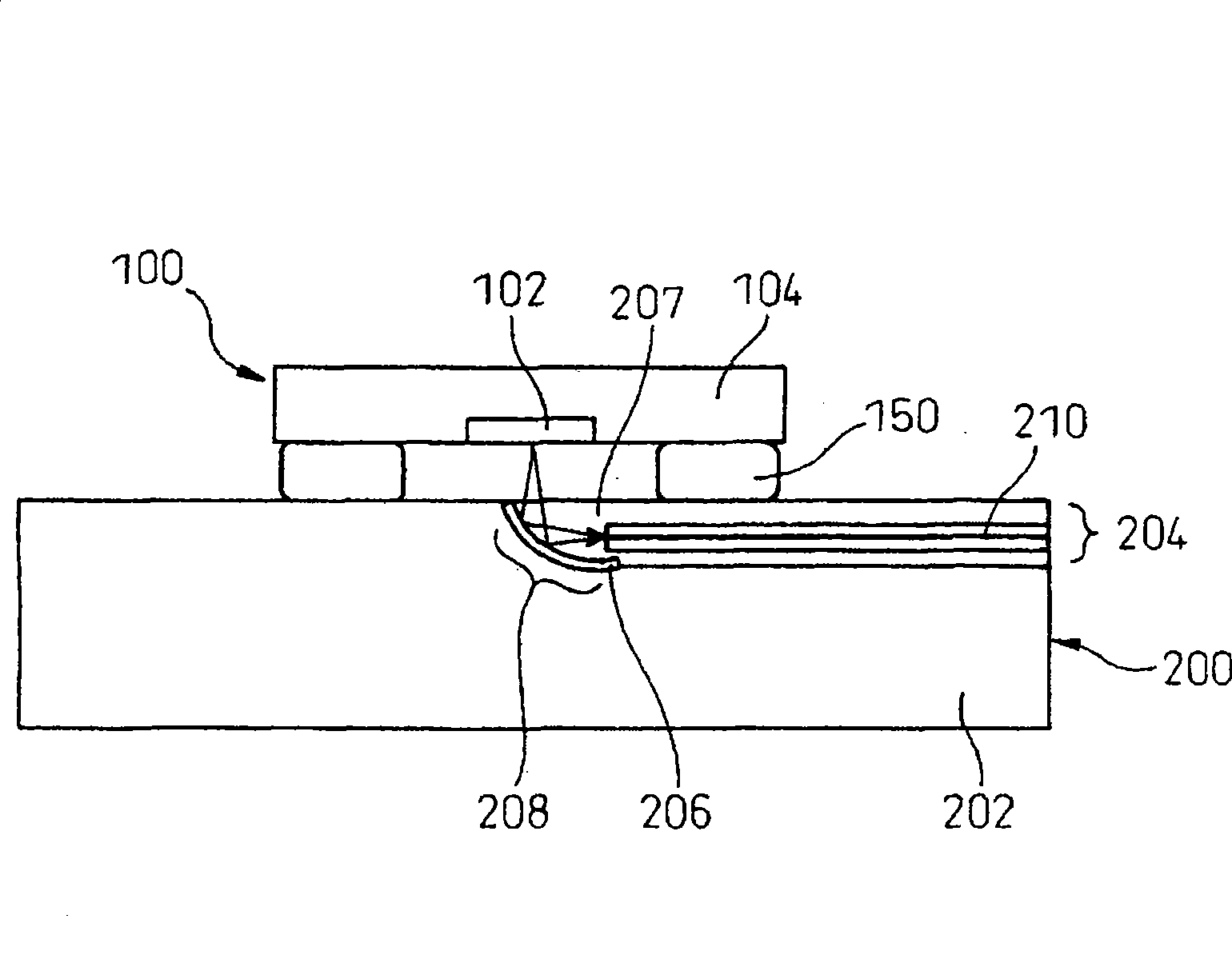
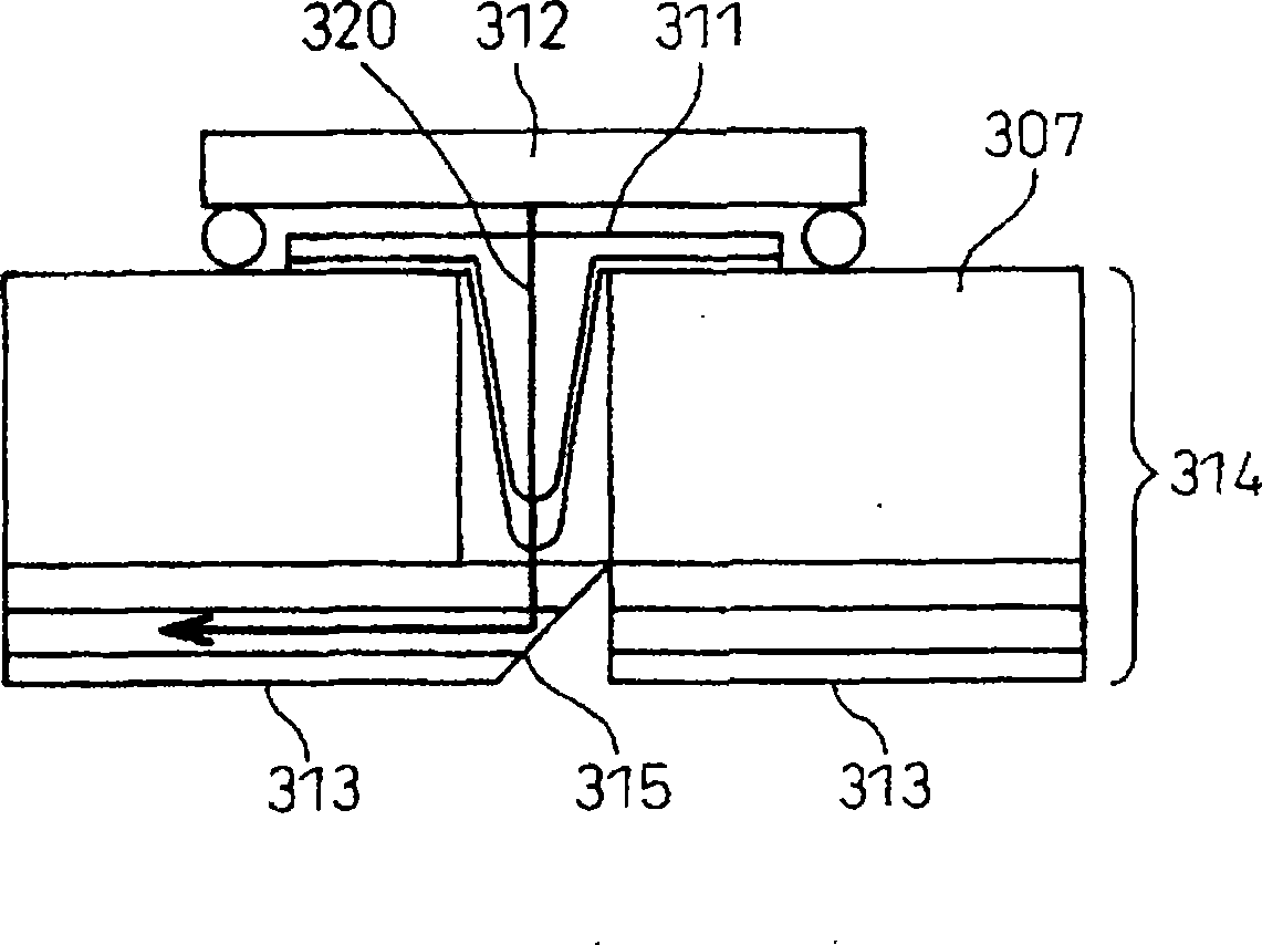
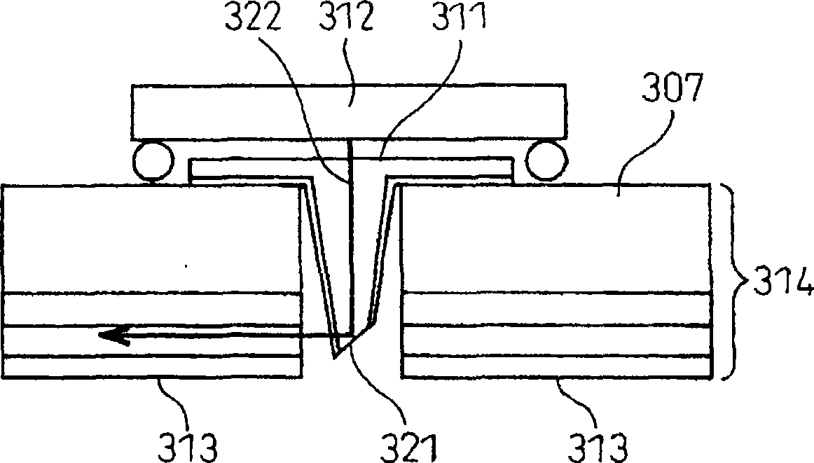
[0041] Figure 3 to Figure 8 A first exemplary embodiment of the present invention is shown. image 3 It is an optical interconnection device on which a substrate with a surface emitting element (hereinafter referred to as "surface emitting element substrate") is mounted. Figure 4 It is a cross-sectional view of an optical / electrical hybrid substrate on which a surface emitting element substrate is mounted. Figure 5 It is a cross-sectional view of an optical / electrical hybrid substrate on which no surface-emitting element substrate is mounted. Image 6 It is a plan view of an optical / electrical hybrid substrate on which no surface emitting element substrate is mounted. Figure 7 is a cross-sectional view of an optical waveguide substrate on which no surface-emitting device substrate is mounted. Figure 8 is a cross-sectional view of an opt...


PUM


Abstract

An optical interconnection device is provided. The optical interconnection device includes an optical component and a substrate on which the optical component is surface-mounted. The substrate includes: an optical waveguide which is formed in the substrate and which includes a core layer, and a cladding layer covering the core layer; and an optical path changing portion provided adjacent to one end portion of the optical waveguide to change an optical path of light transmitted through the optical waveguide or an optical path of light communicated by the optical component. A width of the core layer is broadened toward the optical path changing portion, when viewed from a plane which is parallel with a surface of the substrate.

Description

technical field [0001] The present invention relates to optical interconnect devices. More particularly, the present invention relates to an optical interconnect device on which optical elements such as a light receiving element and a light emitting element are mounted. Background technique [0002] As the signal speed and packaging density of digital devices increase, etc., measures against noise and EMI of electrical signals are required. As such a measure, an optical / electrical hybrid substrate in which a part of electric wiring is replaced with an optical signal is currently being developed. [0003] In the prior art, in the case of mounting optical components such as laser diodes, photodiodes, etc. on optical / electrical hybrid substrates, especially surface mount optical / transmissive) mounted on the substrate, the optical signal will be attenuated due to the optical coupling loss due to the optical axis shift of several micrometers that occurs between the optical wav...

Claims


Application Information

Patent Timeline
Patent Type & Authority Applications(China)
IPC IPC(8): G02B6/42
CPCG02B6/43G02B6/42G02B6/4214H01L2224/16225
Inventor 山本贵功
Owner SHINKO ELECTRIC IND CO LTD
Why Eureka
Try Eureka