Method for producing a multilayered part
A multi-layer, component technology, applied in the direction of thin material handling, transportation and packaging
- Summary
- Abstract
- Description
- Claims
- Application Information
AI Technical Summary
Problems solved by technology
Method used
Image
Examples
example 1
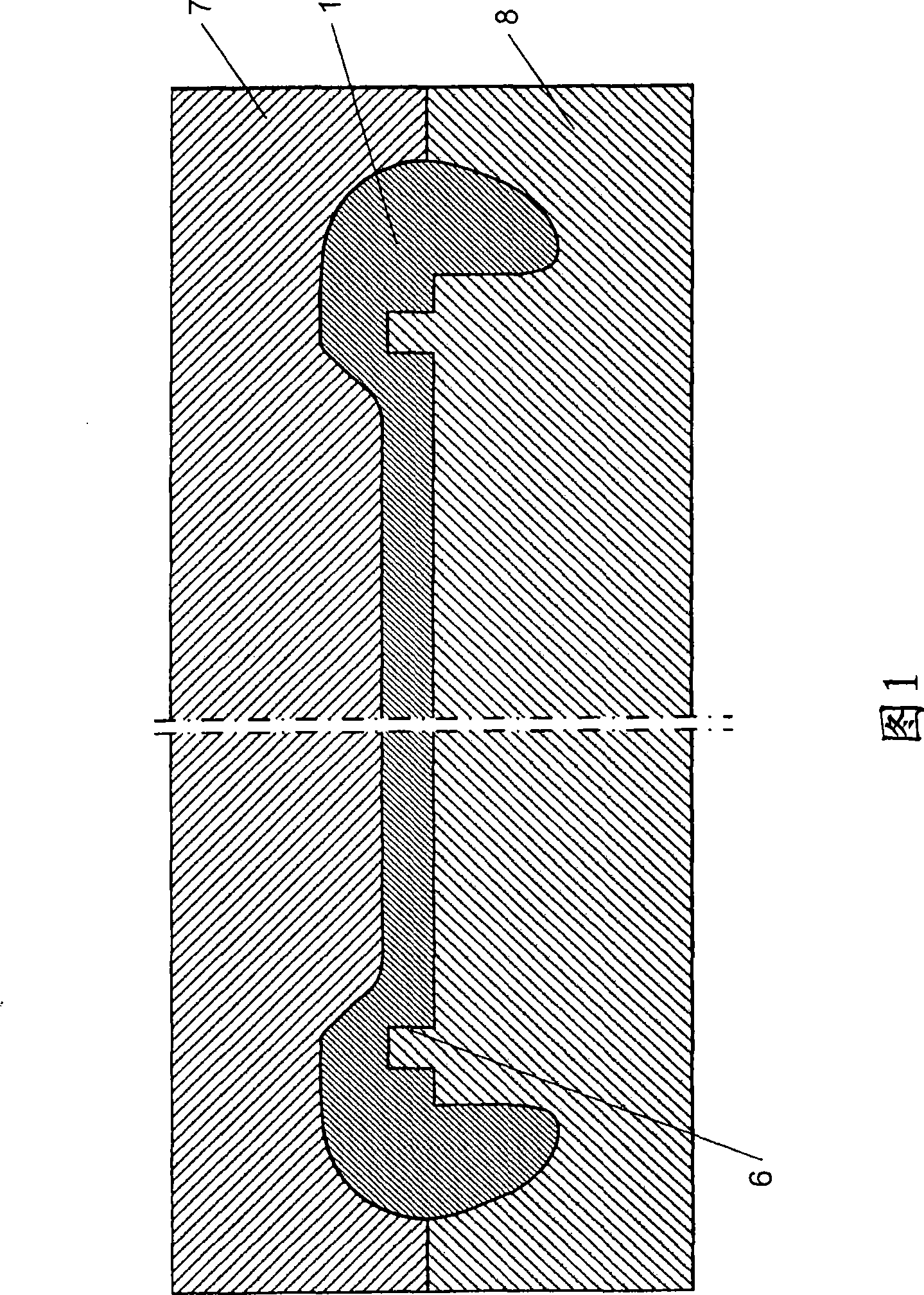
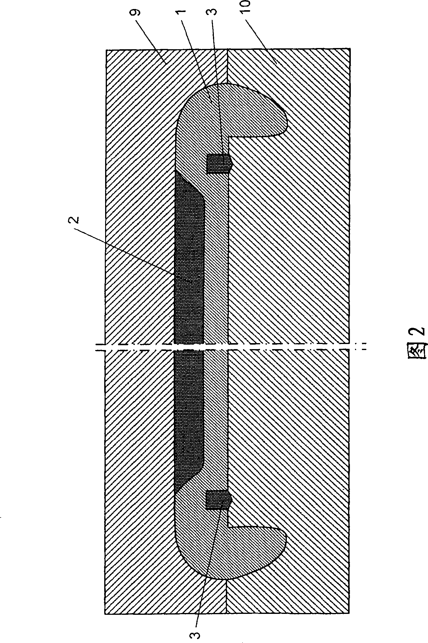
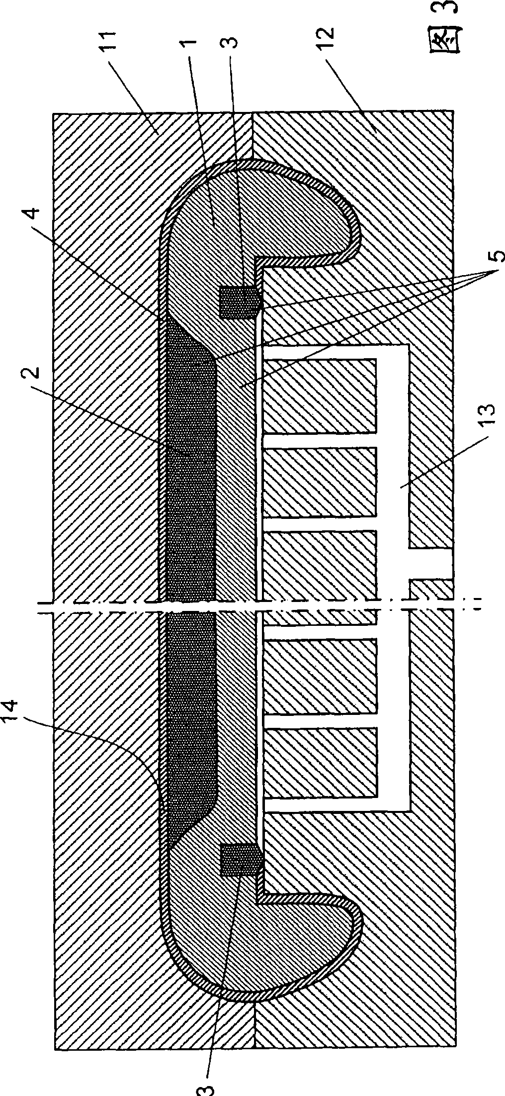
[0042] The PC / ABS base layer was molded by injection molding in the form of a 20 cm x 20 cm panel. One side of this board was overmolded with a layer of SEBS of 6mm thickness. The SEBS layer has about 1000kg / m 3 Density and Shore A hardness of 0. The SEBS layer is then overmolded with a polyurethane reaction mixture to produce a 3 Density polyurethane skin.
[0043] In order to measure the additional softness obtained by the SEBS layer, the ILD (Indentation Load Deflection) value of the multi-layered part was determined, which refers to the need for a 14mm stamping head to punch 2mm of the material at a speed of 5mm / min. force. The same ILD value determination was carried out on a commonly used multilayer part, which included a PC / ABS base layer, a commonly used semi-flexible polyurethane back foam layer (with a thickness of 15mm) and also with a 1.2mm The same polyurethane surface layer of average thickness. The ILD value of the multilayer ROM part measured by the method ...
PUM
| Property | Measurement | Unit |
|---|---|---|
| thickness | aaaaa | aaaaa |
| thickness | aaaaa | aaaaa |
| thickness | aaaaa | aaaaa |
Abstract
Description
Claims
Application Information
 - Generate Ideas
- Intellectual Property
- Life Sciences
- Materials
- Tech Scout
- Unparalleled Data Quality
- Higher Quality Content
- 60% Fewer Hallucinations
Browse by: Latest US Patents, China's latest patents, Technical Efficacy Thesaurus, Application Domain, Technology Topic, Popular Technical Reports.
© 2025 PatSnap. All rights reserved.Legal|Privacy policy|Modern Slavery Act Transparency Statement|Sitemap|About US| Contact US: help@patsnap.com


