Digital phase-locked loop and method for burr elimination
A digital phase-locked loop and order technology, applied in the electronic field, can solve problems such as glitches and achieve the effect of avoiding glitches
- Summary
- Abstract
- Description
- Claims
- Application Information
AI Technical Summary
Problems solved by technology
Method used
Image
Examples
Embodiment 1
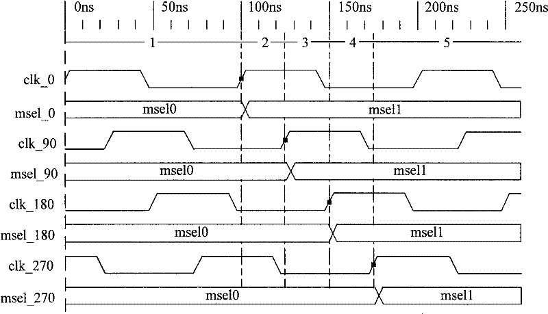
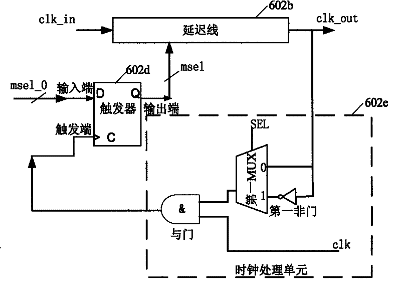
[0044] The embodiment of the present invention provides a digital phase-locked loop, including: MASTER module 601 and SLAVE module 602, and Image 6 The shown digital phase locked loop is similar, MASTER module 601 includes: master clock processing unit 601a, delay line 601b, phase detector 601c and delay control state machine 601d, SLAVE module 602 includes: ratio logic unit 602a, delay line 602b and output Enable unit 602c. and Image 6 The difference of the digital phase-locked loop shown is that the SLAVE module 602 provided in this embodiment also includes a flip-flop 602d connected to the delay line 602b, see Figure 7 ,details as follows:
[0045] The flip-flop 602d is used to use the delayed clock signal clk_out to sample the signal of the first delay unit selection terminal msel_0 in the delay line 602b, and output the sampled signal to the second delay unit selection terminal msel in the delay line . The selection terminal msel_0 of the first delay unit is set to...
Embodiment 2
[0051] The embodiment of the present invention also provides a digital phase-locked loop, including: MASTER module 601 and SLAVE module 602, and Image 6 The same thing as the digital phase-locked loop shown is that the MASTER module 601 includes: a master clock processing unit 601a, a delay line 601b, a phase detector 601c and a delay control state machine 601d, and the SLAVE module 602 includes: a ratio logic unit 602a, a delay line 602b and output enable unit 602c; and Image 6 The difference of the digital phase-locked loop shown is that the SLAVE module 602 provided in this embodiment also includes a flip-flop 602d and a clock processing unit 602e, and the delay unit in the delay line 602b in this embodiment is composed of an OR gate or a NOR gate . see Figure 10 ,details as follows:
[0052] The flip-flop 602d is used to use the delayed clock signal clk_out to sample the signal of the first delay unit selection terminal msel_0 in the delay line 602b, and output the s...
Embodiment 3
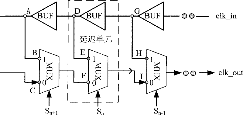
[0062] The embodiment of the present invention also provides a digital phase-locked loop, including: MASTER module 601 and SLAVE module 602, and Figure 10 The difference of the digital phase-locked loop shown is that the SLAVE module 602 provided in this embodiment includes a clock processing unit 602f. In addition to the gate, a second NOT gate is also included, and the delay unit in the delay line 602b in this embodiment is composed of an AND gate or a NAND gate, or is composed of MUX and BUF. see Figure 12 ,details as follows:
[0063] The trigger terminal C of the flip-flop 602d is active at a high level, that is, it is valid after the system clock signal clk is at a low level and the edge of the delayed clock signal clk_out, and other functions are the same as those in Embodiment 2, and the delay line 602b The function is the same as that in Embodiment 2, and will not be repeated here.
[0064] The clock processing unit 602f is configured to perform logic processing ...
PUM
 Abstract
Description
Claims
Application Information
 - R&D
- Intellectual Property
- Life Sciences
- Materials
- Tech Scout
- Unparalleled Data Quality
- Higher Quality Content
- 60% Fewer Hallucinations
Browse by: Latest US Patents, China's latest patents, Technical Efficacy Thesaurus, Application Domain, Technology Topic, Popular Technical Reports.
© 2025 PatSnap. All rights reserved.Legal|Privacy policy|Modern Slavery Act Transparency Statement|Sitemap|About US| Contact US: help@patsnap.com


