Method for processing step ladder PCB plate

A PCB board and processing method technology, applied in the field of stepped PCB board processing, can solve problems such as insufficient glue flow, board size deformation around the groove, etc.

Inactive Publication Date: 2009-01-21
DONGGUAN SHENGYI ELECTRONICS
View PDF0 Cites 9 Cited by
  • Summary
  • Abstract
  • Description
  • Claims
  • Application Information

AI Technical Summary

Problems solved by technology

In the process of PCB board production, the low-flow (LOW-FLOW) prepreg used by the step board to control the flow of glue is prone to local voids in the step layer due to insufficient and uneven flow of glue. Distortion of board dimensions around slots during lamination

Method used


Image

  • Method for processing step ladder PCB plate
  • Method for processing step ladder PCB plate

Examples


Embodiment Construction

[0014] The present invention will be described in detail below in conjunction with the accompanying drawings.

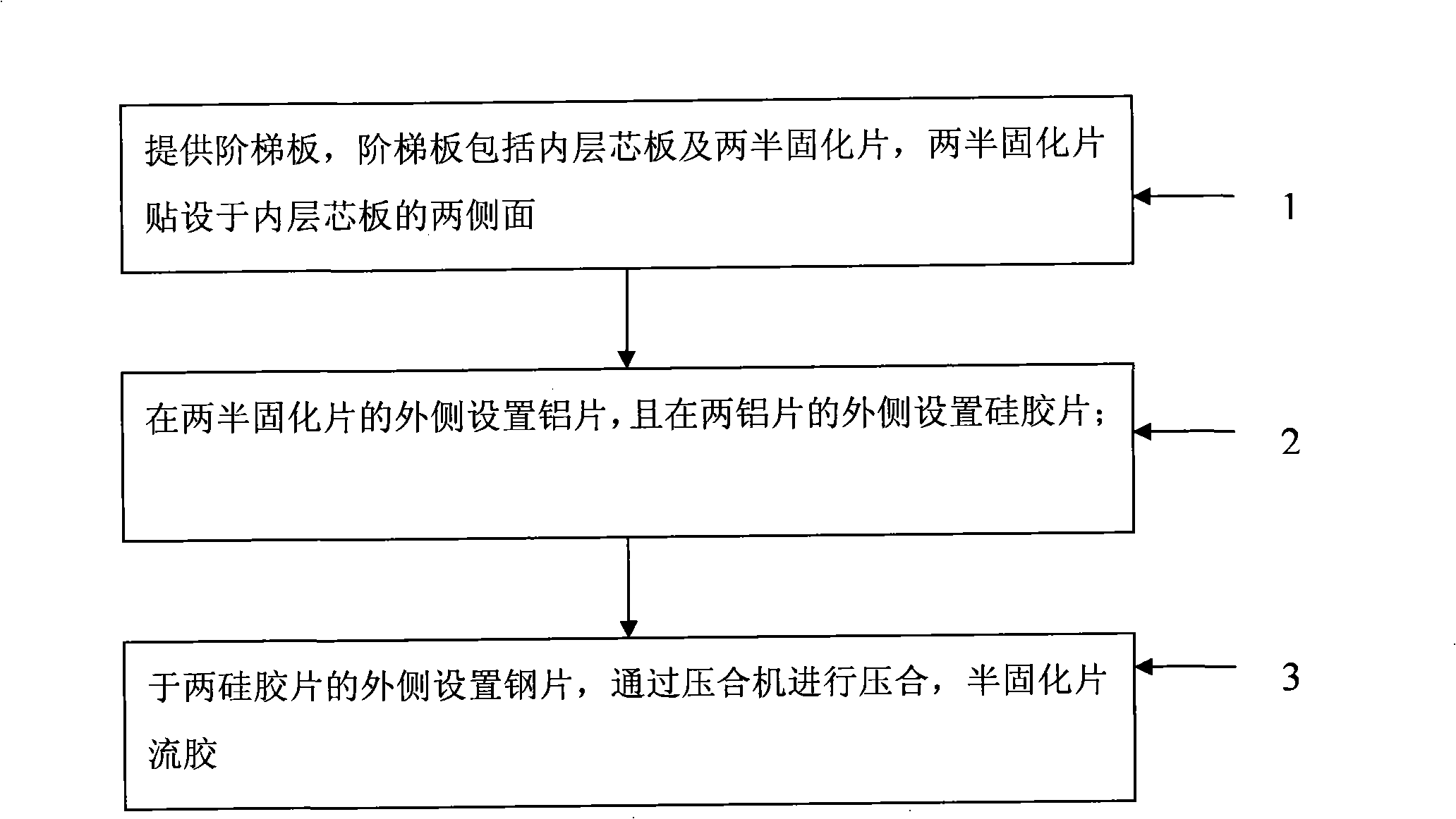
[0015] Such as figure 1 Shown, the processing method of ladder PCB board of the present invention, comprises the following steps:

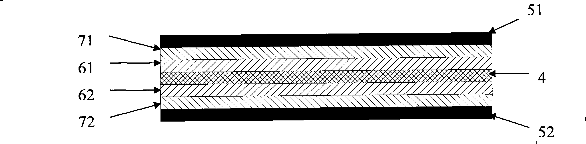
[0016] Step 1: Provide a stepped board. The stepped board includes an inner core board and two prepregs. The two prepregs are attached to both sides of the inner core board; There is a stepped groove, and the prepreg is set corresponding to the inner core board. It is a low-fluidity prepreg, and a suitable prepreg is selected to ensure the glue flow at the location of the stepped groove.

[0017] Step 2: Set aluminum sheets on the outside of the two prepregs, and set silica gel sheets on the outside of the two aluminum sheets; in this step, use the silica gel sheet with cushioning properties to cover the prepreg flow glue of the step plate in the lamination process Adjustment, so that the flow glue of the stepped plate is evenly distri...


PUM


Abstract

The invention relates to a method for processing a ladder PCB plate, which includes the following steps: a ladder plate is provided and comprises an inner layer core plate and two prepregs which are attached to the two sides of the inner layer core plate; silicon rubber slices are arranged at the external sides of two aluminum sheets which are arranged at the external sides of the two prepregs; steel sheets which are arranged at the external sides of the two silicon rubber slices are pressed by a pressing machine and the gummosis is carried out for the prepregs. By arranging the aluminum sheets and silicon rubber slices in the laminating process, the method for processing the ladder PCB plate leads the gummosis of the ladder plate to be distributed evenly to avoid the local cavity of the ladder plate with the help of the cushioning property of the silicon rubber slices; at the same time, the combination mode of the aluminum sheets and the silicon rubber slices is adopted to reduce the level tensile force imposed to a ladder groove by the silicon rubber slices so as to avoid the risk of deformation in the laminating process, caused by the middle suspension of the ladder groove and the ladder PCB plate manufactured is caused to have good qualified rate and excellent performance.

Description

technical field [0001] The invention relates to the field of printed circuit board manufacture, in particular to a method for processing a stepped PCB board. Background technique [0002] Due to the rapid development of electronic technology, the continuous development of printed circuit board (PCB) technology has been promoted. In the process of PCB board production, the low-flow (LOW-FLOW) prepreg used by the step board to control the flow of glue is prone to local voids in the step layer due to insufficient and uneven flow of glue. Dimensional deformation of the board around the groove during lamination. Contents of the invention [0003] The object of the present invention is to provide a method for processing a stepped PCB board, which uses the cushioning characteristics of "aluminum sheet + silica gel sheet" to solve the cavity and slot deformation of the stepped board. [0004] In order to achieve the above object, the present invention provides a method for proce...

Claims


Application Information

Patent Timeline
Patent Type & Authority Applications(China)
IPC IPC(8): H05K1/09B32B37/02B32B37/15B32B37/10B32B15/04
Inventor 杜红兵
Owner DONGGUAN SHENGYI ELECTRONICS
Why Eureka
Try Eureka