Method for Fe doped growing GaFeN dilution magnetic semiconductor and uses thereof

A magnetic semiconductor and synthesis method technology, applied in the application of magnetic films to substrates, semiconductor/solid-state device manufacturing, magnetic layers, etc., to achieve fast data processing capabilities and low power consumption

Active Publication Date: 2012-07-04
NANJING UNIV
View PDF0 Cites 0 Cited by
  • Summary
  • Abstract
  • Description
  • Claims
  • Application Information

AI Technical Summary

Problems solved by technology

In this way, the intrinsic magnetism of GaN-based dilute magnetic semiconductor materials needs to be further confirmed by experiments

Method used


Image

  • Method for Fe doped growing GaFeN dilution magnetic semiconductor and uses thereof
  • Method for Fe doped growing GaFeN dilution magnetic semiconductor and uses thereof
  • Method for Fe doped growing GaFeN dilution magnetic semiconductor and uses thereof

Examples


Embodiment Construction

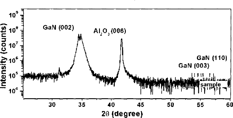
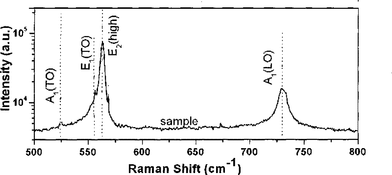
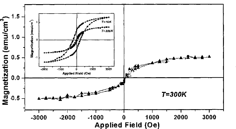
[0022] The invention utilizes MOCVD growth technology, adopts sapphire substrate and Fe doping technology, directly high-temperature nitriding the substrate material and then growing low-temperature GaN and high-temperature GaN buffer layer technology, and then on the GaN buffer layer through Fe doping control synthesis growth GaFeN Technology for diluting magnetic semiconductor thin film materials. Through the selection and control of process parameters such as the growth temperature of different growth layers and the flow control of the growth source, the GaFeN diluted magnetic semiconductor thin film material is synthesized and grown. It includes the following steps:

[0023] 1) Using MOCVD growth technology, using sapphire substrate and Fe doping technology, directly high-temperature nitriding the substrate material and then growing low-temperature GaN and high-temperature GaN buffer layer two-step technology, and then through Fe doping control on the GaN buffer layer Synthe...


PUM


Abstract

The invention provides a method for synthesizing the growth of a GaFeN diluted magnetic semiconductor thin-film material by Fe doping. The method adopts an MOCVD growth method, and comprises the following steps of: (1) nitridizing a substrate material at a high temperature on a sapphire substrate, and passing through H2, N2 or gas of H2 and N2 in an MOCVD growth system to carry out a substrate surface treatment on the sapphire substrate at a temperature of between 1,000 and 1,100 DEG C; (2) growing a low-temperature GaN buffer layer; (3) growing a high-temperature GaN buffer layer, with a thickness between 0.5 and 2um; and (4) synthesizing the growth the GaFeN diluted magnetic semiconductor thin-film material through Fe doping control on the high-temperature GaN buffer layer, and passing through ammonia, trimethyl gallium and dicyclopentadienyl iron (CP2Fe) with flow ranges of between 0.1 and 5slm, between 1 and 10sccm and between 15 and 200sccm respectively at a temperature of between 900 and 1,150 DEG C to grow the GaFeN diluted magnetic semiconductor thin-film material, and maintaining pressure of a growth chamber between 5 and 500Torr.

Description

Technical field [0001] The invention relates to a method for growing GaFeN diluted magnetic semiconductors by Fe-doping using metal organic chemical vapor phase epitaxial growth technology (MOCVD), in particular to using MOCVD technology to grow GaFeN diluted magnetic semiconductors on a sapphire substrate material through Fe-doping growth technology Methods of semiconductor thin film materials. The Fe-doped diluted magnetic semiconductor material GaFeN film grown by the method can be used in spintronic devices. The advantages of this device are faster data processing capabilities, low power consumption and other potentially unprecedented advantages. On it, different epitaxial structures can be grown according to different device applications, such as spin field effect tubes, spin light emitting diodes, quantum computing and other fields. The invention can effectively control the growth of GaFeN materials. Obtained GaFeN diluted magnetic semiconductor film material with obvio...

Claims


Application Information

Patent Timeline
Patent Type & Authority Patents(China)
IPC IPC(8): H01L21/205C30B29/38C30B25/00C30B25/18H01F1/10H01F10/18H01F41/22
Inventor 谢自力张荣陶志阔崔旭高陈鹏修向前韩平赵红刘斌李弋宋黎红崔颖超施毅郑有炓
Owner NANJING UNIV
Why Eureka
Try Eureka