Method and subassembly for testing two-sided chip photoelectric performance

A technology for photoelectric performance and testing components, which is applied in the direction of testing optical performance, measuring electricity, and measuring electrical variables, etc. It can solve problems such as inaccurate, unrealizable, chip damage, etc., and achieve the effect of ensuring repeatability and accuracy

Inactive Publication Date: 2008-08-13
SUZHOU INST OF NANO TECH & NANO BIONICS CHINESE ACEDEMY OF SCI
View PDF0 Cites 10 Cited by
  • Summary
  • Abstract
  • Description
  • Claims
  • Application Information

AI Technical Summary

Problems solved by technology

[0005] However, when testing the optical performance of double-sided chips, the above-mentioned testing methods have great limitations.
[0006] Because for a double-sided device, it is necessary to introduce light from one side and prick the needle from the other side to lead to the electrode. In ordinary detection devices, the light source and the probe are set on the same side, so this function cannot be realized; Chip pricking has the following disadvantages:
[0007] (1) Use the probe to prick the needle directly on the device. If the electrode is too small, it is easy to pierce inaccurately;
[0008] (2) For the same device, since the orientation of each needle injection and the size of the needle injection force are different, it will also bring problems of accuracy and repeatability;
[0009] (3) Needling directly will destroy the electrode of the chip and cause damage to the chip

Method used


Image

  • Method and subassembly for testing two-sided chip photoelectric performance
  • Method and subassembly for testing two-sided chip photoelectric performance
  • Method and subassembly for testing two-sided chip photoelectric performance

Examples


Embodiment 1

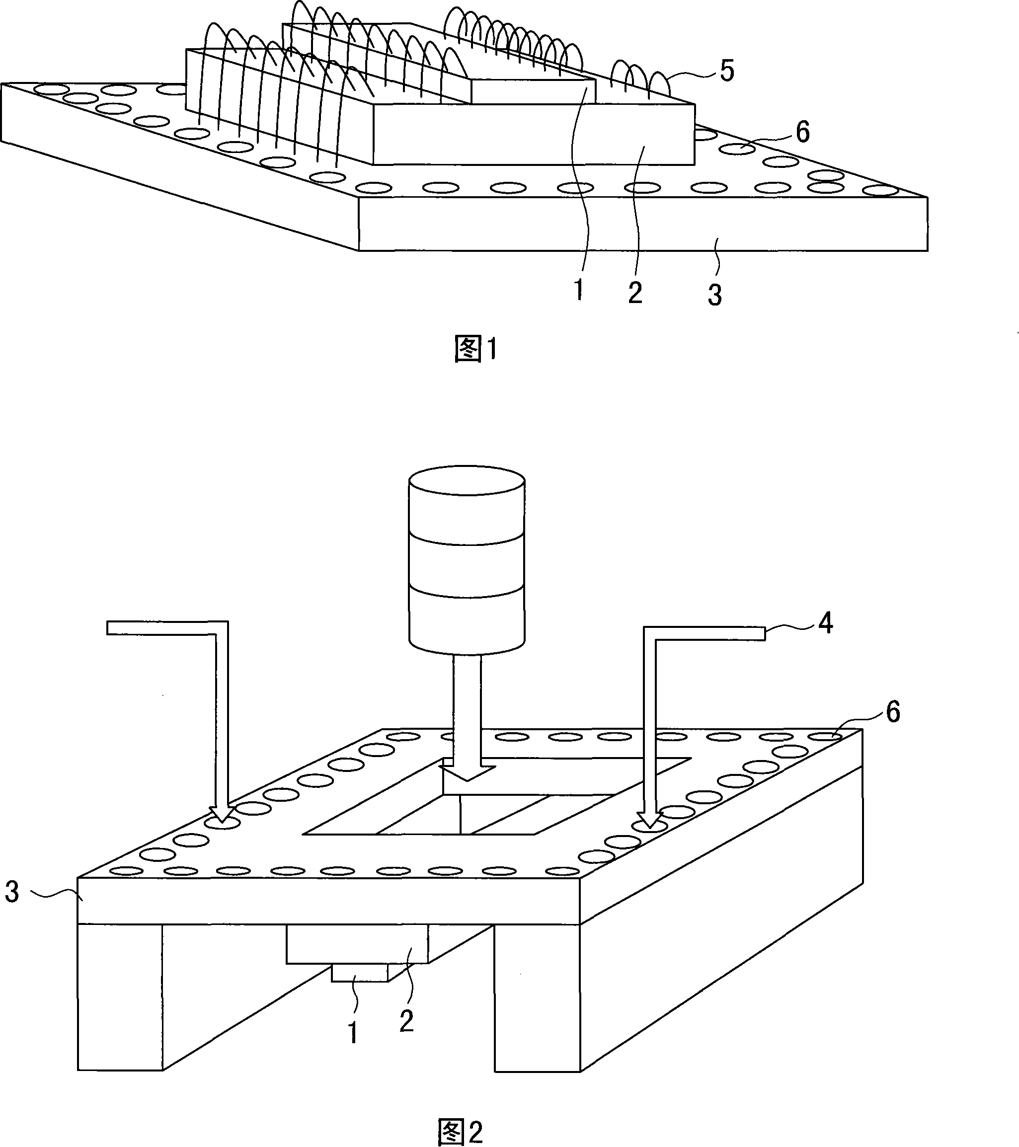
[0032] Embodiment one, see accompanying drawing 1~4 shown:

[0033] A method for testing the photoelectric performance of a double-sided chip, comprising the following steps:

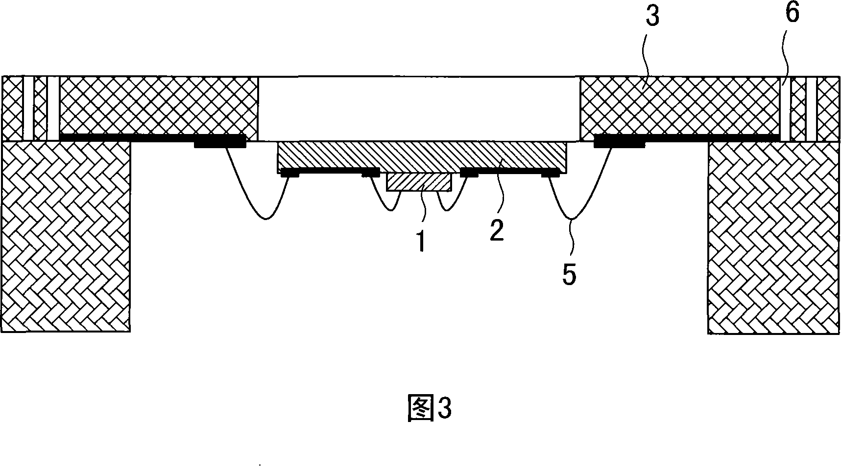
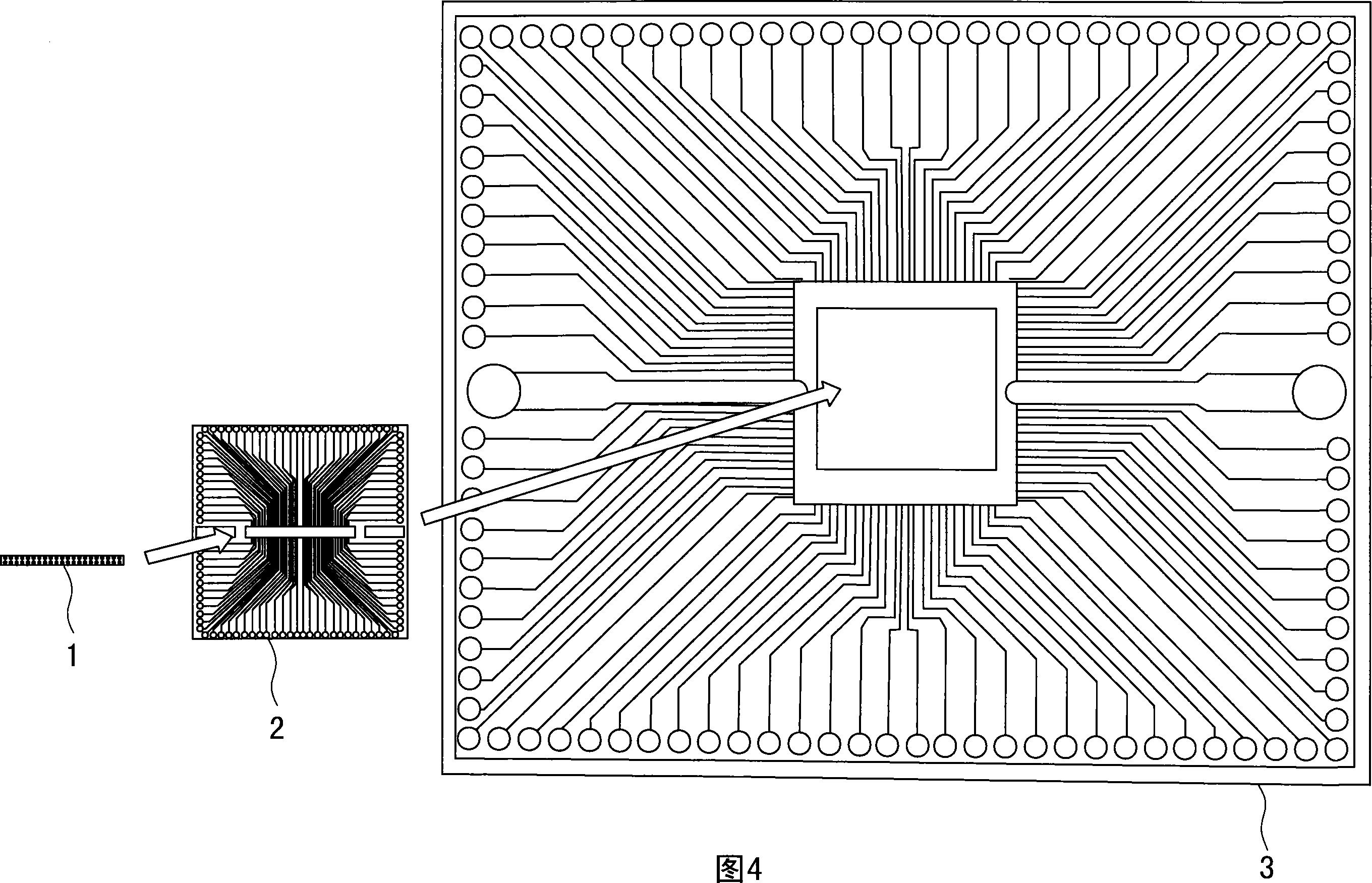
[0034] (1) Build a test assembly, the test assembly includes a printed circuit board 3 that is provided with a lead-out circuit corresponding to the electrode of the double-sided chip 1 to be tested, and the light-receiving position of the printed circuit board 3 is corresponding to the double-sided chip 1 to be tested. Each electrode of the double-sided chip 1 to be tested is electrically connected to the corresponding lead-out circuit on the printed circuit board 3 through a gold wire 5 connection, and a test electrode 6 is arranged at the end of each lead-out circuit;

[0035] (2) above-mentioned test assembly is placed on the test frame, and the test light is irradiated on the light-receiving position of the double-sided chip to be tested through the hole on the printed circuit board; each probe 4 i...


PUM


Abstract

The invention discloses a component for testing double-faced chip photoelectric properties, comprising a to-be tested double-faced chip; one side of the double-faced chip is equipped with photic position; another side is equipped with pins. Said component also comprises a glass substrate and a printing circuit board. Said printing circuit board is equipped with through holes. The photic side of said to-be tested double-faced chip is fixedly connected to the glass substrate. The glass substrate is fixedly connected to the printing circuit board; said printing circuit board is equipped with the leading circuits. Each leading circuit is respectively equipped with testing electrodes. Each electrode of said to-be tested double-faced chip is respectively connected to corresponding transition circuits via golden line; each transition circuit is respectively connected to corresponding leading circuit via golden line. This invention also discloses a method for using the component to test double-faced chip photoelectric properties; said component not only can achieve photoelectric properties test of the double-faced chip, but also it endures accuracy and repeatability of the test.

Description

technical field [0001] The invention relates to the field of optical testing of chip micro-regions, in particular to a device and method for testing the photoelectric performance of a double-sided chip. Background technique [0002] In the field of semiconductors, optoelectronic performance testing of manufactured optical devices is required. Usually, the test device adopts a probe station structure, including a positioning motor, a testing machine, a probe, a light source and a bracket part. Both the light source and the probe are set on the front of the device under test. The lead-out electrode is pricked to realize the measurement of the photoelectric performance of the device. When testing single-sided chips, the following steps are usually included: [0003] (1) Place the chip to be tested on the bracket so that the light receiving window or photoelectric sensing area on the front of the chip to be tested is aligned with the incident direction of the light source; by ...

Claims


Application Information

Patent Timeline
Patent Type & Authority Applications(China)
IPC IPC(8): G01M11/00G01M11/02G01R31/00G01R31/28G01R31/308
Inventor 黄寓洋杨晨刘楠张耀辉
Owner SUZHOU INST OF NANO TECH & NANO BIONICS CHINESE ACEDEMY OF SCI
Why Eureka
Try Eureka