
Multiple inlet atomic layer deposition reactor

A technology of atomic layer deposition and reactor, applied in coating, metal material coating process, semiconductor/solid-state device manufacturing, etc., can solve complex problems

Active Publication Date: 2008-04-30
ASM GENITECH KOREA
View PDF4 Cites 17 Cited by
  • Summary
  • Abstract
  • Description
  • Claims
  • Application Information

AI Technical Summary

Problems solved by technology

The loop can also be more complex

Method used


Image

  • Multiple inlet atomic layer deposition reactor
  • Multiple inlet atomic layer deposition reactor
  • Multiple inlet atomic layer deposition reactor

Examples


Embodiment Construction

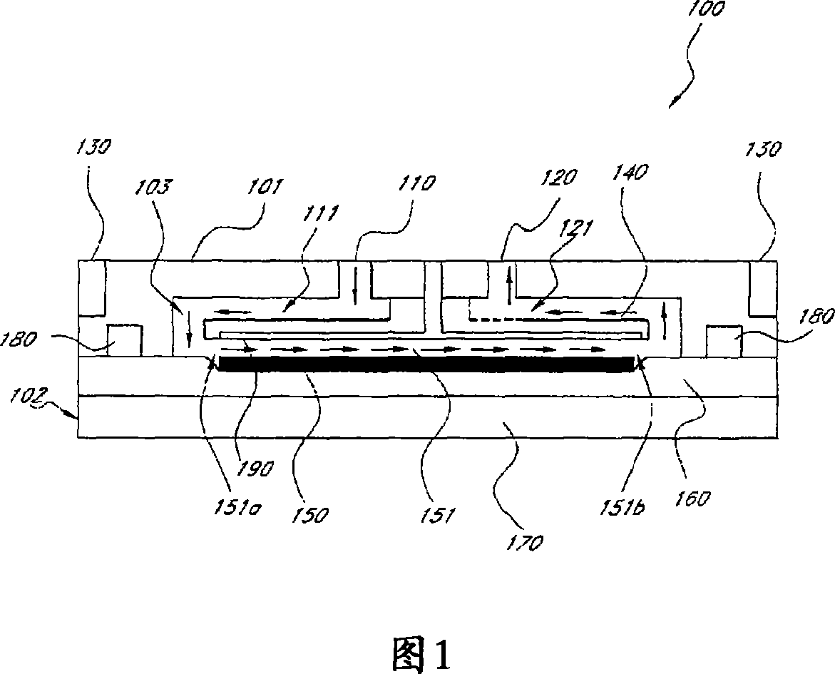
[0019] Figure 1 shows an ALD reactor suitable for sequential introduction of reactants into a reaction space, similar to the reactor disclosed in US Patent No. 6,539,891. In FIG. 1 , a reactor 100 includes a reactor cover 101 , a reactor base 102 and a gas flow control plate 140 .

[0020] The reactor cover 101 constitutes the upper part of the reactor 100 and has a short cylindrical structure with the top closed. The reactor cover 101 includes a reactant inlet 110 and an outlet 120 . A portion of the side wall of the reactor lid 101 is surrounded by the lid heater 130 .

[0021] The reactor base 102 is located below the reactor cover 101 . The reactor base 102 can move vertically relative to the reactor cover 101 . When the reactor base 102 is separated from the reactor cover 101, the substrate 150 can be loaded or unloaded. For deposition, the reactor base 102 is moved upwards and brought into sealing contact with the reactor lid 101 . The reactor base 102 is configured...


PUM


Abstract

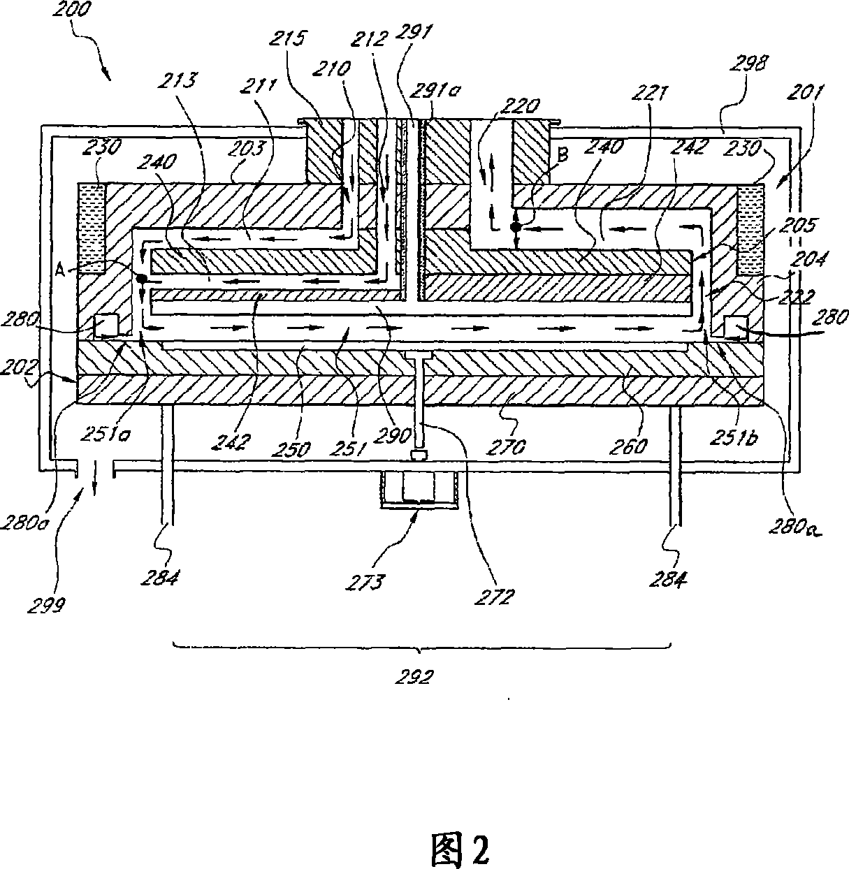
A reactor (200) configurated to subject a substrate to alternately repeated surface of vapophase reactants is disclosed. The reactor includes a reaction chamber, a plurality of inlets (210,212), and an exhaust outles (220). The reaction chamber includes a reaction space (251). The reactor also includes a gas flow control guide structure (205) within the reaction chamber. The gas flow control guide structures (205) sides over the reaction space (251) and is interposed between the plurality of inlets (210,212) and the reaction space. The gas flow control guide structure (205) includes a plurality of channels (210,212), and each of the channels extends form one of the inlets to an upstream periphery of the reaction space. Each of the channels progressively widens as the channel extends form the inlet to the reaction space (251). The reacto further includes a substrate holder (260) in the reaction space (251).

Description

technical field [0001] The invention relates to a device for growing thin films on the surface of a substrate. More specifically, the present invention relates to an apparatus for producing a thin film on the surface of a substrate by subjecting the substrate to alternating and repeated surface reactions of gas phase reactants. Background technique [0002] This application claims priority from Korean Patent Application No. 2005-0038606 filed with the Korean Intellectual Property Office on May 9, 2005, the disclosure of which is hereby incorporated by reference. This application is also related to US Patent No. 6,539,891, issued April 1, 2003, entitled "CHEMICALDEPOSITION REACTOR AND METHOD OF FORMING ATHIN FILM USING THE SAME," the disclosure of which is hereby incorporated by reference. [0003] In the production of semiconductor devices, various methods and apparatuses have been developed for providing high quality thin films on substrates. Several methods using surface...

Claims


Application Information

Patent Timeline
Patent Type & Authority Applications(China)
IPC IPC(8): C23C16/00
CPCC23C16/45548C23C16/5096C23C16/45591C23C16/4554C23C16/4412C23C16/45519H01L21/10
Inventor 金大渊李政镐刘龙珉
Owner ASM GENITECH KOREA
Learn More