


Quick Research
Generate reliable direction feasibility study reports for your R&D in just a few steps.

Technical Q&A
Discover and master advanced knowledge NOW. Basics, ideas, possibilities, all at once.

Find Solutions
As an expert in R&D theories, this can generate solutions to your technical problems instantly.

Evaluate Feasibility
Analyze your overall solution with one click, know your potential R&D risks in advance.

Monitor Landscape
Get weekly tech updates, stay abreast of the latest tech innovations and key insights.
Mosfet with temperature sense facility
A sensing and gate technology, applied in the field of FET, can solve the problem of difficult integration of MOSFET
- Summary
- Abstract
- Description
- Claims
- Application Information
AI Technical Summary
Problems solved by technology
Method used
Image


Examples
Embodiment Construction
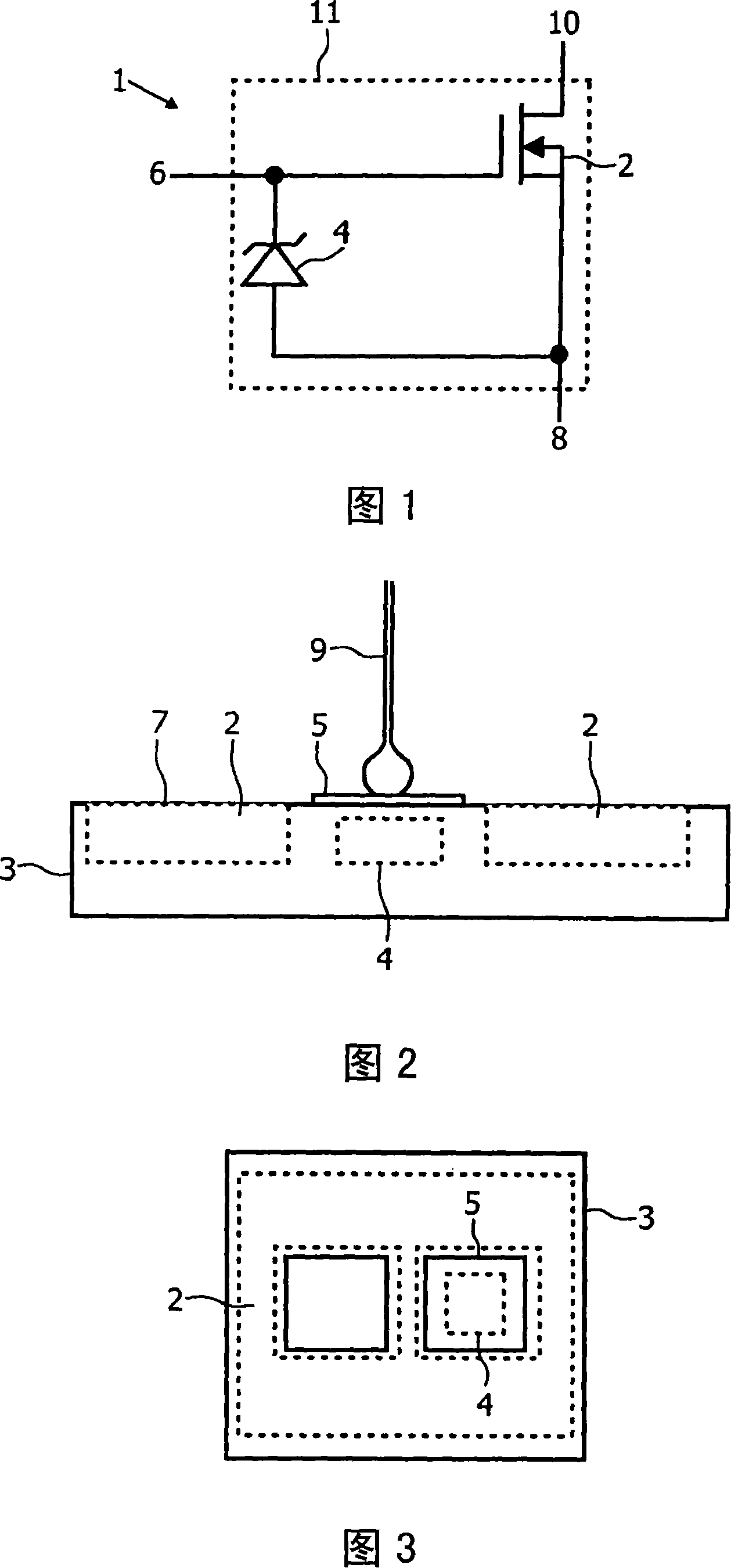
[0039] Referring to Figures 1-3, Figure 1 schematically illustrates a transistor device with a temperature sensing arrangement. 2 and 3 show a semiconductor substrate in top and side views.
[0040] A Field Effect Transistor (FET) 2 transistor region is provided on a semiconductor substrate 3, known as Field Effect Transistor Region 2 defining source, gate and drain regions. Any suitable transistor FET structure may be used, including horizontal and vertical structures.
[0041] The Zener diode 4 is electrically connected between the gate and the source of the FET 2, the cathode of the diode is connected to the gate of the FET 2, and the anode of the diode is connected to the source of the FET 2, as shown in FIG. 1 .
[0042] Although a single diode 4 is shown, multiple diodes in series oriented in the same direction could be used instead.
[0043] In FIGS. 2 and 3 a spatial arrangement is shown in which a gate bonding pad 5 and a bonding wire 9 are provided on a first main ...
PUM
 Abstract
Description
Claims
Application Information
 - R&D Engineer
- R&D Manager
- IP Professional
- Industry Leading Data Capabilities
- Powerful AI technology
- Patent DNA Extraction
Browse by: Latest US Patents, China's latest patents, Technical Efficacy Thesaurus, Application Domain, Technology Topic, Popular Technical Reports.
© 2024 PatSnap. All rights reserved.Legal|Privacy policy|Modern Slavery Act Transparency Statement|Sitemap|About US| Contact US: help@patsnap.com