Universal asynchronous serial extended chip of multi-bus interface
A universal asynchronous and serial port expansion technology, which is applied in the field of universal asynchronous serial port expansion chips with multi-bus interfaces, can solve the problems of slow communication speed, complicated operation and high cost, and achieve the effect of reducing the burden
- Summary
- Abstract
- Description
- Claims
- Application Information
AI Technical Summary
Problems solved by technology
Method used
Image
Examples
Embodiment 1
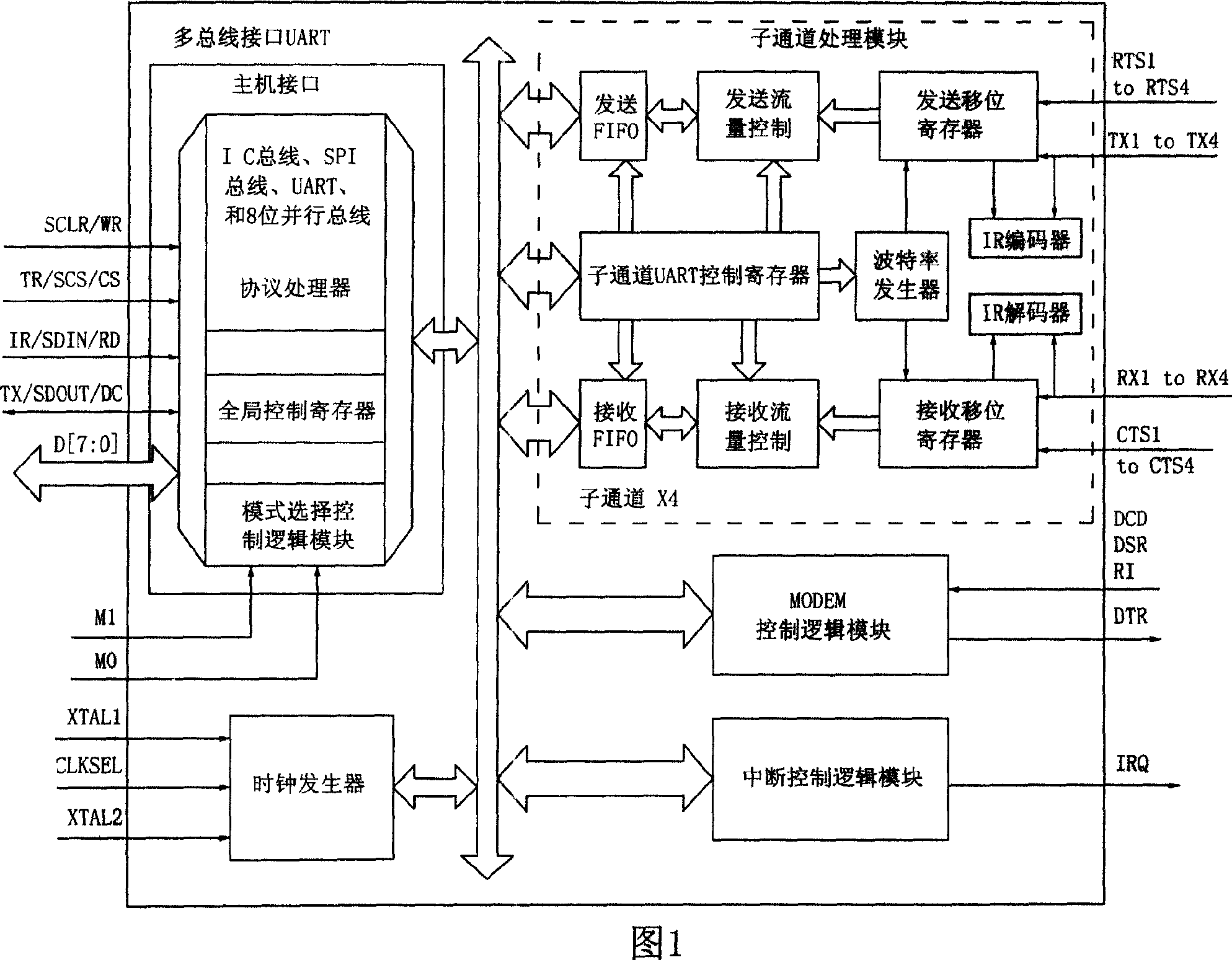
[0048] As shown in Figure 1, a universal asynchronous serial port expansion chip with multiple bus interfaces includes a host interface, a sub-channel processing module, a MODEM control logic module, an interrupt control logic module, and a clock generator. The host interface includes an 8-bit parallel bus. Interface, serial peripheral interface SPI bus interface, UART bus interface, internal integrated circuit bus I 2 C bus interface, protocol processor, global register, and mode selection control logic module; the four bus interfaces are all connected to the CPU / DSP host, the bus type corresponding to the host is selected through the bus processing logic, and the SPI, SPI, and SPI are processed through the bus processing logic. UART, I 2 The unified conversion of the data and data format of C and 8-bit parallel buses; the global register setting sets the working state of the chip host interface; the mode selection control logic module selects the host interface through the mode ...
Embodiment 2
[0061] A universal asynchronous serial port expansion chip with multi-bus interface. This chip adopts a simplified register structure. The register is numbered according to the address as a 6-bit address number, and the address is 000000~111111.
[0062] The host interface of the chip includes RSV, global control register GCR, global main serial port control register GMUCR, global interrupt register GIR, global XOFF character register GXOFFH and global XON character register GXON, a total of 6 global registers.
[0063] The address of the global register is XX0000-XX0101, where XX is any one of 00, 01, 10, 11, the upper 2 bits are the channel number, the lower 4 bits are the register address number, and the lower 4 bits of the address are arranged in detail See the table below:
[0064] The global register list is as follows:
[0065] Register address[3:0]
Register name
Types of
Register function description
(XX)0000
RSV
No
Keep
(XX)...
Embodiment 3
[0109]The chip in the present invention supports a data broadcast mode in which the sub-serial channel can be independently configured. By setting the GBDEN bit in the global register GCR, the global broadcast of the master port is set to enable, and then the RDBEN bit of the SCTLR of the corresponding sub serial channel that needs to receive broadcast data is set, so that the channel can receive data broadcast. After the main interface control logic detects the broadcast setting, it sends the data of the main port to all the sub-serial ports. The broadcast data can be set to receive the sub-serial port that is enabled to receive the broadcast, but the sub-serial port that is not set to receive data broadcast will ignore the data. . So as to realize the data broadcasting function that can be independently configured.
PUM
 Abstract
Description
Claims
Application Information
 - R&D
- Intellectual Property
- Life Sciences
- Materials
- Tech Scout
- Unparalleled Data Quality
- Higher Quality Content
- 60% Fewer Hallucinations
Browse by: Latest US Patents, China's latest patents, Technical Efficacy Thesaurus, Application Domain, Technology Topic, Popular Technical Reports.
© 2025 PatSnap. All rights reserved.Legal|Privacy policy|Modern Slavery Act Transparency Statement|Sitemap|About US| Contact US: help@patsnap.com


